Three-dimensional stacking encapsulation method based on silicon through-hole

A packaging method and three-dimensional stacking technology, applied in semiconductor devices, electrical components, circuits, etc., can solve problems such as through-hole voids, high through-hole resistance, premature sealing, etc., to simplify packaging steps, improve reliability, and uniform density. Effect

Inactive Publication Date: 2010-04-14
SEMICON MFG INT (SHANGHAI) CORP +1
View PDF2 Cites 0 Cited by
  • Summary
  • Abstract
  • Description
  • Claims
  • Application Information

AI Technical Summary

Problems solved by technology

Using the above packaging method requires the step of depositing copper seeds, and the process is more complicated; and the uniformity of copper seed deposition has a great influence on electroplating, and the process requirements are very high; in addition, when electroplating through holes with a large depth-to-width ratio, the opening is easy Premature sealing will cause holes in the through holes. The resistance of the through holes formed in this way is high, and the substances remaining in the holes during electroplating may be corrosive, which will affect the reliability of the through holes.

Method used


Image

  • Three-dimensional stacking encapsulation method based on silicon through-hole
  • Three-dimensional stacking encapsulation method based on silicon through-hole
  • Three-dimensional stacking encapsulation method based on silicon through-hole

Examples


Embodiment Construction

[0012] An embodiment of the TSV-based three-dimensional stack packaging method of the present invention is described below with reference to the accompanying drawings, in order to further understand the purpose, specific structural features and advantages of the present invention.

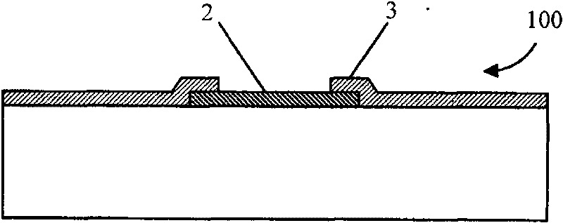
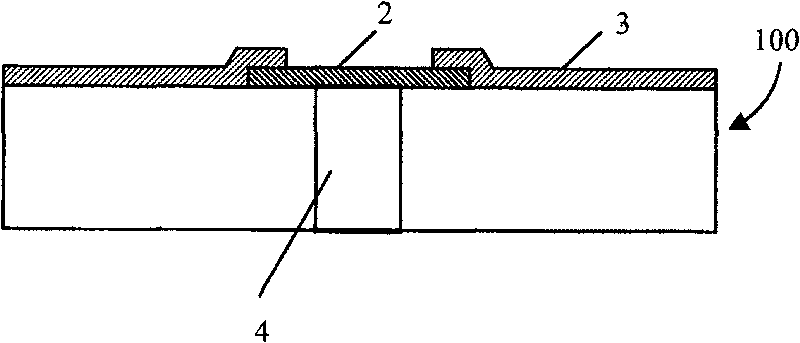
[0013] see figure 1 , the package-on-package method of the present invention includes the following steps. Firstly, several wafers to be packaged are provided. Since the steps of making TSVs are the same for each wafer, the description of the following steps takes the wafer 100 as an example. The front side of the wafer 100 has several welding pads 2 , a barrier layer (silicon dioxide) 3 is deposited on the front side of the wafer 100 , and then an etching step is performed to expose the welding pads 2 . see figure 2 , plate photoresist (not shown) on the back of the wafer, perform photolithography (exposure, development) steps, form photolithographic patterns, and then use Deep Reactive Etch (D...


PUM


Abstract

The invention discloses a three-dimensional stacking and packaging method based on silicon through-holes, and relates to an integration technology in the semi-conductor field. The method comprises thefollowing steps: wafers to be packaged are provided, and each wafer is provided with a plurality of welding pads; etching process is carried out for blocking layers deposited on the faces of the wafers until the welding pads on the wafers are exposed; silicon through-holes are formed in positions corresponding to the welding pads; electrodeless plating is adopted for filling the silicon through-holes with metal, and ends of through-holes filled with the metal are electrically connected with the welding pads, and the other ends thereof extend from the backs of the wafers to form connection parts; electrodeless plating is used for plating the welding pads with metal, and the plated metal protrudes from the faces of the wafers to form connection parts; and wafer bonding equipment is utilizedfor bonding the connection part onto the face of one wafer with the connection part on the back of another wafer, and then stacking the two connection parts up. Compared with the prior art, in the method provided by the invention, the electrodeless plating technology is adopted for filling the silicon through-holes with the metal, thereby simplifying the packaging process and improving the reliability of the stacked wafers.

Description

technical field [0001] The invention relates to the integration technology in the field of semiconductors, in particular to a three-dimensional stack packaging method based on through-silicon vias. Background technique [0002] Consumer products, such as digital cameras, PDAs and mobile phones, and next-generation servers have higher and higher requirements for product miniaturization: functionality needs to be enhanced, storage capacity must be increased, and the package shape of memory and processors must be reduced. In order to meet this requirement, many device manufacturers have begun to study three-dimensional interconnection technology to stack chips. [0003] At present, the three-dimensional stack packaging technology based on copper-filled silicon vias has been widely used in the production process of semiconductors. The three-dimensional packaging method based on copper-filled TSVs generally includes the following steps: forming TSVs; depositing a barrier layer (...

Claims


Application Information

Patent Timeline
Patent Type & Authority Patents(China)
IPC IPC(8): H01L21/60
CPCH01L2224/16145
Inventor 靳永刚毛剑宏朱文渊章国伟
Owner SEMICON MFG INT (SHANGHAI) CORP
Why Eureka
Try Eureka