

Gallium nitride semiconductor device with improved termination scheme
a technology of gallium nitride and semiconductor devices, which is applied in the direction of semiconductor devices, diodes, electrical devices, etc., can solve the problems of inconvenient provision of reliable guard rings such as p-type guard rings, the inability to control the manufacturing process, and the inability to provide convenient guard rings. reliable, the effect of improving the structural integrity
- Summary
- Abstract
- Description
- Claims
- Application Information
AI Technical Summary
Benefits of technology
Problems solved by technology
Method used
Image

Examples
Embodiment Construction
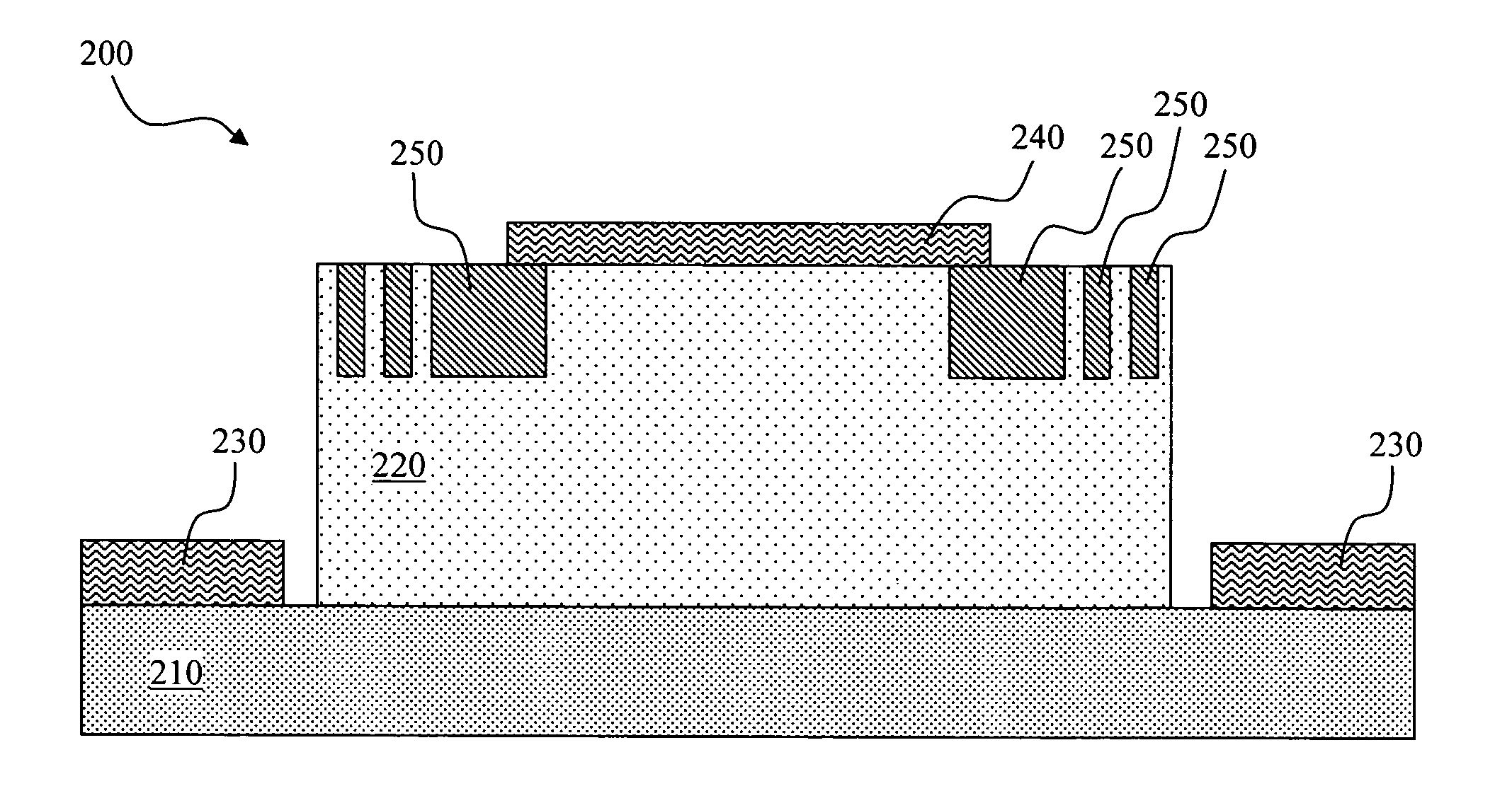
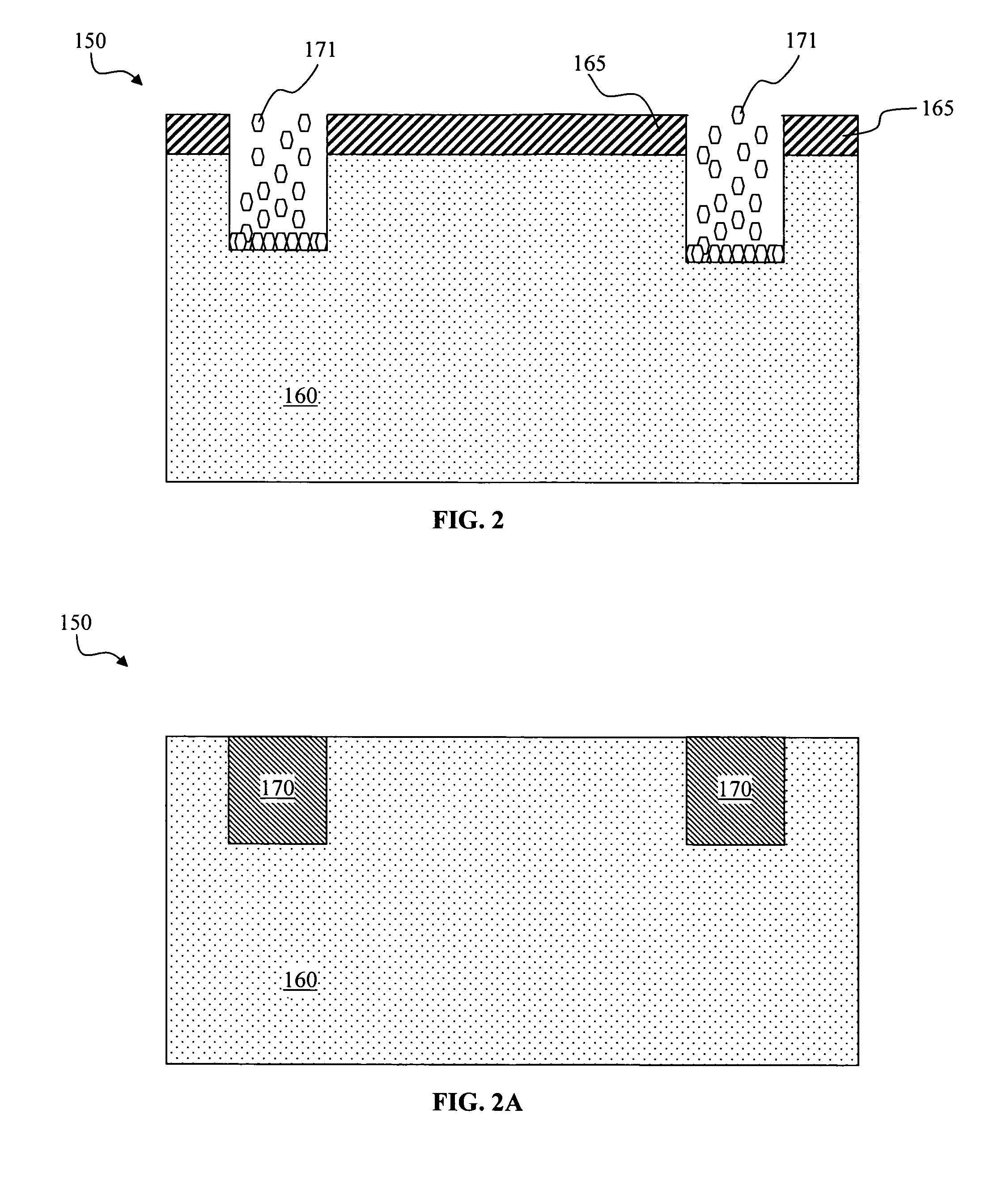
[0021]Refer to FIGS. 2 and 2A for a cross sectional view of a semiconductor device 150. The detailed configurations of the device 150 are not specifically shown here. The semiconductor device 150 includes an N-type Gallium nitride layer 160. The semiconductor device 150 further includes termination structures with p-type guard rings 170 formed by selective epitaxial growth 171. The epitaxial growth 171 is shown in FIG. 2, while the completed p-type guard rings are shown in FIG. 2A. By epitaxially growing the P-type GaN, the P-type guard rings 170 are formed having high quality and true P-type. As will be further described below the p-type guard rings are formed by applying a re-growth mask 165 to open trenches in the GaN layer 160. Then guard rings 170 are formed by epitaxial growth 171 in these trenches followed by removal of the regrowth mask 165 and a chemical mechanical planarization (CMP) process to planarize the p-type guard rings 170 complete the processes of forming the term...
PUM
 Abstract
Description
Claims
Application Information