Supercharge Your Innovation With Domain-Expert AI Agents!

Fin structure and method of manufacturing fin transistor adopting the fin structure

一种鳍式结构、结晶的技术,应用在半导体/固态器件制造、电固体器件、半导体器件等方向,能够解决鳍式结构成本高、鳍式结构均匀性降低等问题

Inactive Publication Date: 2008-02-13
SAMSUNG ELECTRONICS CO LTD
View PDF1 Cites 2 Cited by
  • Summary
  • Abstract
  • Description
  • Claims
  • Application Information

AI Technical Summary

Problems solved by technology

In these conventional methods, due to the narrow line width, the uniformity of the fin structure is reduced, and the cost of manufacturing the fin structure is high

Method used


Image

  • Fin structure and method of manufacturing fin transistor adopting the fin structure
  • Fin structure and method of manufacturing fin transistor adopting the fin structure
  • Fin structure and method of manufacturing fin transistor adopting the fin structure

Examples


Embodiment Construction

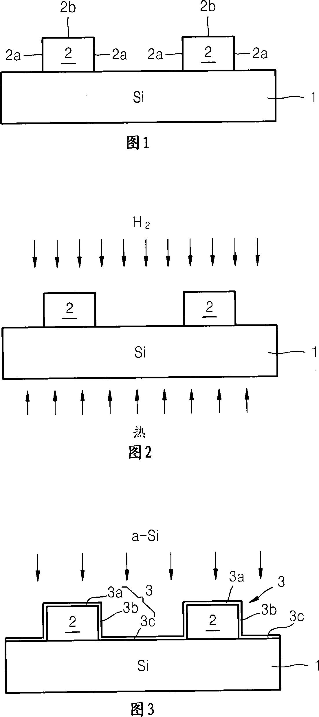
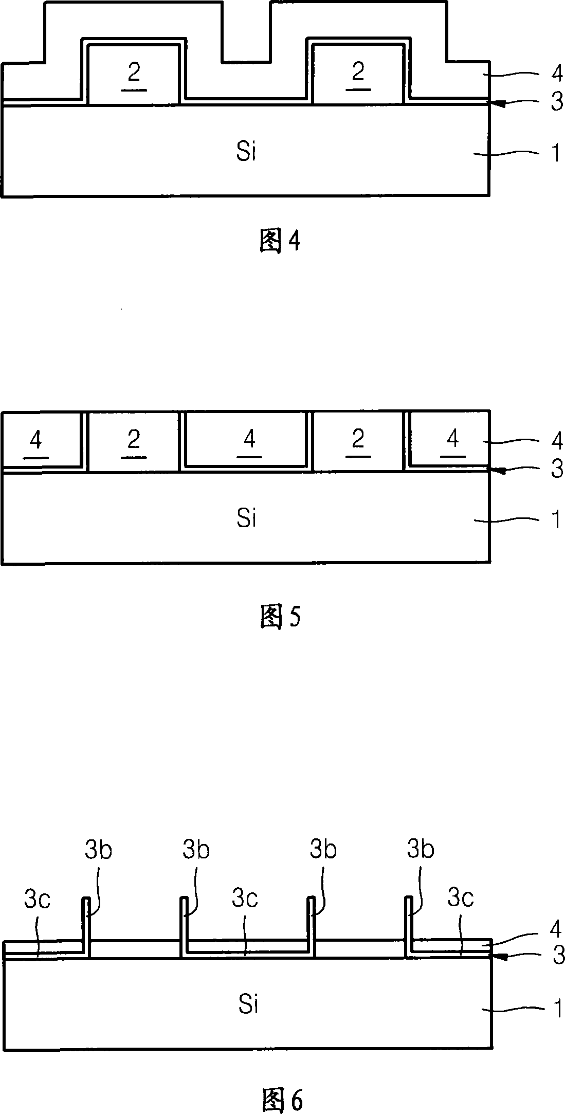
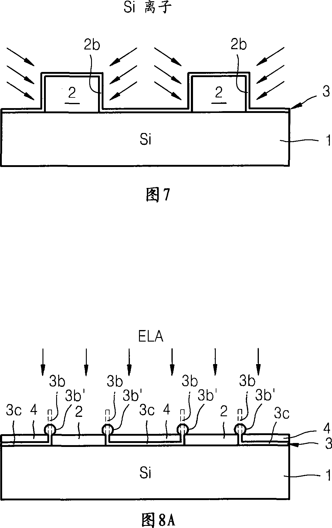
[0019] A method of manufacturing a fin structure according to the present invention will now be described with reference to the accompanying drawings. This method corresponds to the method of manufacturing a fin-type active region of a fin-type transistor. Therefore, the method of manufacturing a fin transistor according to the present invention will be easily understood from this method.

[0020] 1 to 6 are cross-sectional views illustrating a process of manufacturing a fin structure according to an embodiment of the present invention. In the embodiments of the present invention, silicon will be described as an application of a material forming a semiconductor layer.

[0021] As shown in FIG. 1 , a plurality of mesa structures 2 having a predetermined length are formed on a silicon substrate 1 . The mesa structure 2 has an upper surface 2b and side surfaces 2a formed beside the upper surface 2b. The distance between the mesa structures 2 must be properly adjusted according...


PUM


Abstract

Provided are a fin structure and a method of manufacturing a fin transistor adopting the fin structure. A plurality of mesa structures including sidewalls are formed on the substrate. A semiconductor layer is formed on the mesa structures. A capping layer is formed on the semiconductor layer. Thus, the semiconductor layer is protected by the capping layer and includes a portion which is to be formed as a fin structure. A portion of an upper portion of the capping layer is removed by planarizing, and thus a portion of the semiconductor layer on upper surfaces of the mesa structures is removed. As a result, fin structures are formed on sides of the mesa structures to be isolated from one another. Therefore, a fin structure having a very narrow width can be formed, and a thickness and a location of the fin structure can be easily controlled.

Description

technical field [0001] The present invention relates to a method of manufacturing a fin structure, and more particularly, to a method of manufacturing a fin transistor used in a semiconductor memory device. Background technique [0002] Fin transistors are suitable for 100nm or smaller design rules (design rule). In particular, fin transistors have been studied as low-power, high-efficiency, and high-speed devices. An active region with a line width of 20nm or less is extremely required to obtain full depletion of the fin transistor. In order to obtain a fin transistor satisfying such requirements, it is very important to fabricate a fin structure as an active region. [0003] Traditionally, sidewall techniques, ultraviolet lithography, electron beam lithography, etc. are used to form the fin structure. A known method is to form a polysilicon fin structure on a silicon substrate using sidewall technology. US Patent Application Publication No. 2005-0048727 discloses a met...

Claims


Application Information

Patent Timeline
Patent Type & Authority Applications(China)
IPC IPC(8): H01L21/02H01L21/336
CPCH01L29/785H01L27/1052H01L29/66795H01L27/105H01L21/8239H10B99/22H01L21/18
Inventor 赵世泳朴永洙鲜于文旭
Owner SAMSUNG ELECTRONICS CO LTD
Features
  • R&D
  • Intellectual Property
  • Life Sciences
  • Materials
  • Tech Scout
  • Unparalleled Data Quality
  • Higher Quality Content
  • 60% Fewer Hallucinations
Learn More