A silicon slice deviation dynamic regulation method and device by photoelectric switch

A photoelectric switch, silicon wafer technology, applied in circuits, electrical components, transportation and packaging, etc., can solve problems such as affecting the silicon wafer process, complex operating procedures, and inability to guarantee silicon wafers.

Active Publication Date: 2008-07-09
BEIJING NAURA MICROELECTRONICS EQUIP CO LTD
View PDF0 Cites 14 Cited by
  • Summary
  • Abstract
  • Description
  • Claims
  • Application Information

AI Technical Summary

Problems solved by technology

During the transfer of silicon wafers, often due to problems such as control, the silicon wafers cannot be transferred to the designated location
Especially in the transmission process of 300 mm silicon wafers, it is necessary to transport the silicon wafers from the transmission chamber to the reaction chamber. During the transportation process, the manipulator may sometimes have the center position deviation or drop of the silicon wafers, so that it is impossible to guarantee whether the silicon wafers are It can be accurately centered on the reactive electrostatic chuck, which will seriously affect the subsequent process of silicon wafers
In the traditional sol

Method used


Image

  • A silicon slice deviation dynamic regulation method and device by photoelectric switch
  • A silicon slice deviation dynamic regulation method and device by photoelectric switch
  • A silicon slice deviation dynamic regulation method and device by photoelectric switch

Examples


Embodiment Construction

[0019] The following examples are used to illustrate the present invention, but are not intended to limit the scope of the present invention.

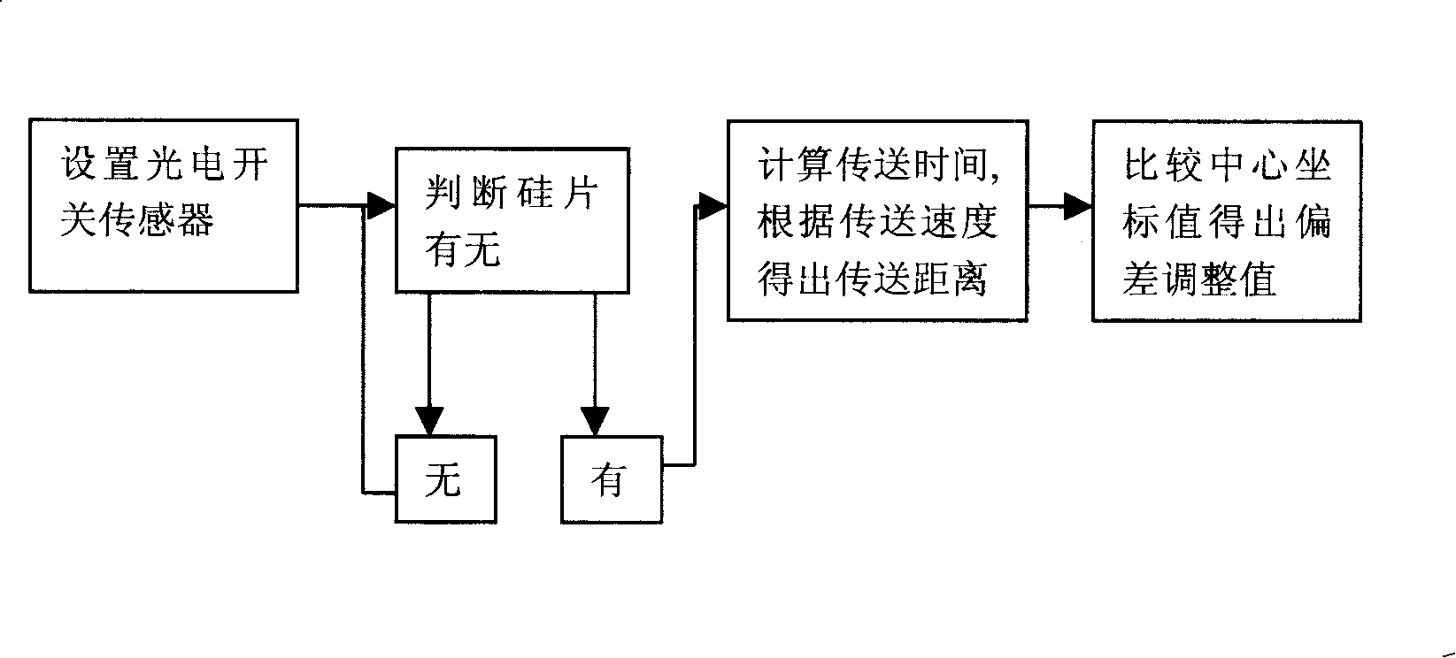
[0020] Basic detection principle: such as figure 1 As shown, in the process of the manipulator transporting the silicon wafer from the transfer chamber to the reaction chamber, the transfer time of the silicon wafer is judged by the photoelectric switch sensor 1, and the running distance is calculated by combining the average speed of the manipulator to obtain the current silicon wafer on the manipulator. The center coordinate of the chip is compared with the center coordinate value of the silicon chip when there is no deviation, and the difference obtained is the required deviation adjustment value.

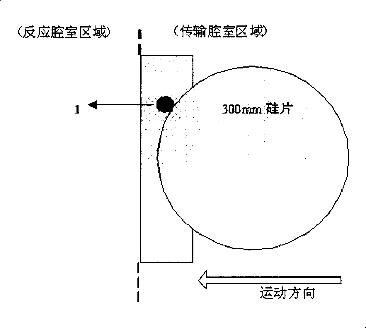
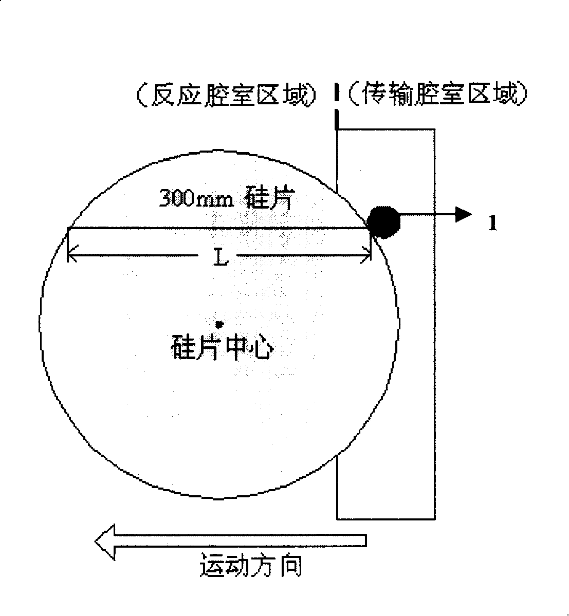
[0021] Device layout: as figure 2 , Figure 4 As shown, the photoelectric switch sensor 1 is located off-center at the connection between the transfer chamber and the reaction chamber, and the manipulator is used to transport the sili...


PUM


Abstract

The invention relates to the field of the adjustment technology of a silicon wafer and provides a method and a device to use a photoelectric switch for dynamic adjustment of the deviation of the silicon wafer. The basic detection principle of the method is that: in the process of using a mechanical hand to deliver the silicon wafer to a reaction chamber from a transfer chamber, the transfer time of the silicon wafer is judged by a photoelectric switch sensor, and the operation distance is calculated by the combination of the average motion speed of the mechanical hand, so as to obtain the center coordinate of the silicon wafer on the current mechanical hand, the comparison of the value and the center coordinate of the silicon wafer without the deviation is carried out, and the obtained value difference is the deviation adjustment value which is needed. The invention has the advantage and the beneficial effect of accurately calculating the position of the deviation of the silicon wafer and guiding the mechanical hand to adjust the deviation of the silicon wafer automatically.

Description

technical field [0001] The invention relates to the technical field of silicon chip adjustment, in particular to a method and device for dynamically adjusting silicon chip deviation by a photoelectric switch. Background technique [0002] In the modern silicon wafer manufacturing process, due to the different processing procedures and processing environments involved, the silicon wafer needs to be transferred. During the transfer of silicon wafers, often due to problems such as control, the silicon wafers cannot be transferred to the designated location. Especially in the transmission process of 300 mm silicon wafers, it is necessary to transport the silicon wafers from the transmission chamber to the reaction chamber. During the transportation process, the manipulator may sometimes have the center position deviation or drop of the silicon wafers, so that it is impossible to guarantee whether the silicon wafers are It can be accurately centered on the reactive electrostatic...

Claims


Application Information

Patent Timeline
IPC IPC(8): H01L21/68H01L21/677
Inventor 李永军
Owner BEIJING NAURA MICROELECTRONICS EQUIP CO LTD
Why Eureka
Try Eureka