

Electronic component mounting system and electronic component mounting method
一种电子元件安装、电子元件的技术,应用在用电元件组装印刷电路、电气元件、电气元件等方向,能够解决不能有效地执行安装位置修正、焊料位置信息不能被利用等问题
Active Publication Date: 2008-11-26
PANASONIC CORP
View PDF1 Cites 35 Cited by
- Summary
- Abstract
- Description
- Claims
- Application Information
AI Technical Summary
Problems solved by technology
For this reason, solder position information acquired by a print inspection device may not be available, and thus mounting position correction may not be effectively performed during component mounting
Method used
View moreImage
Smart ImageViewing Examples

Examples
Embodiment Construction
Login to View More PUM
 Abstract
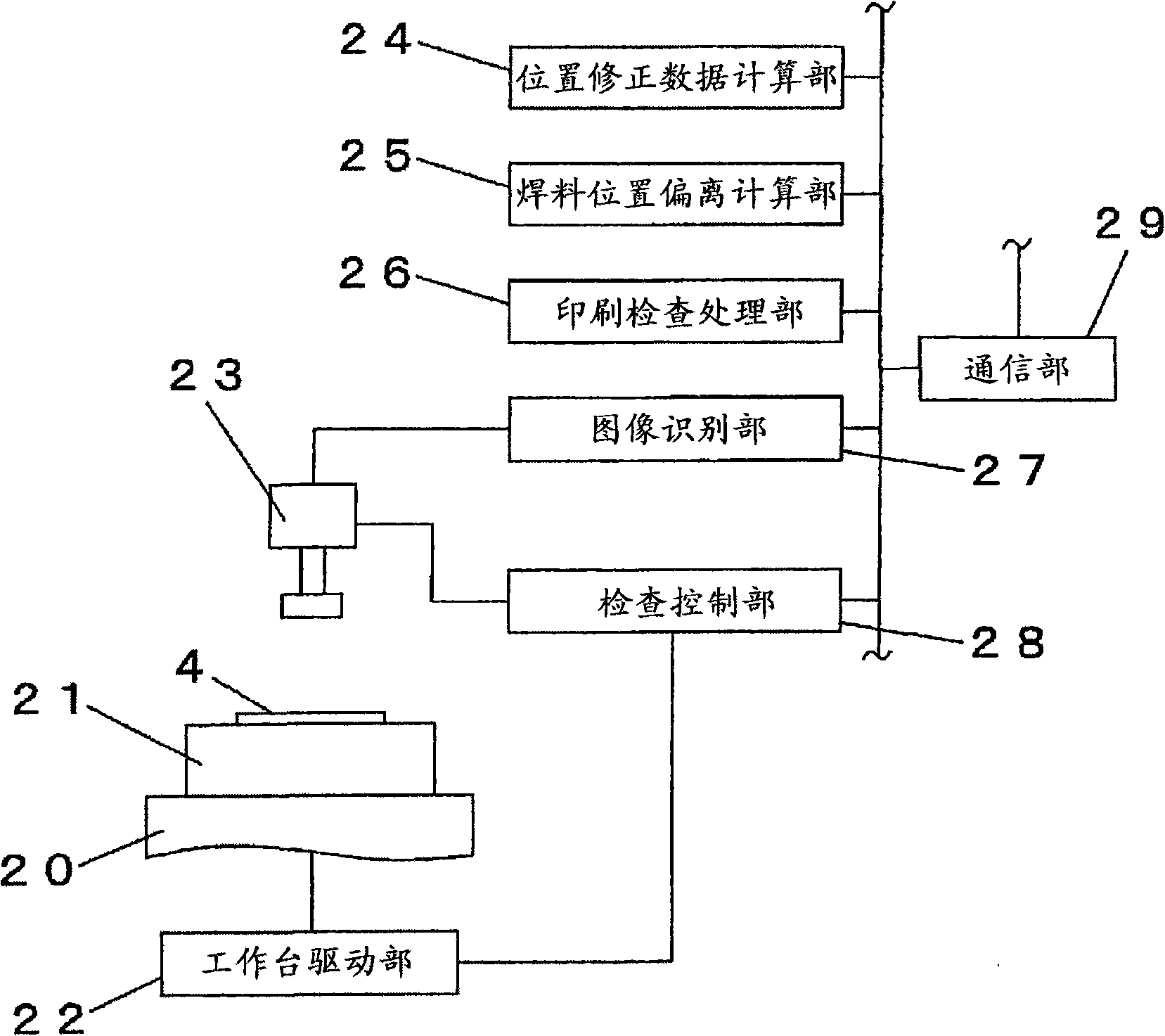
In electronic component mounting for a plurality of individual substrates held on a carrier, solder position deviation data is calculated for each individual substrate based on a mark position recognition result on a carrier after solder printing, a solder position recognition result, and electrode position information indicating the position of an electrode on each individual substrate, an operation of calculating position correction data, which is used to correct the positional deviation to mount electronic components at proper positions, is performed for each individual substrate based on the calculated solder position deviation data and the calculated position correction data is feed-forwarded to an electronic component mounting apparatus, and an electronic component mounting operation of a component mounting mechanism is controlled based on the mark position recognition result and the position correction data.
Description
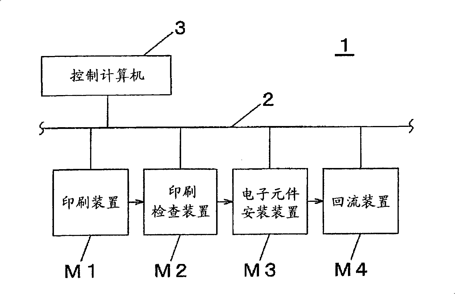
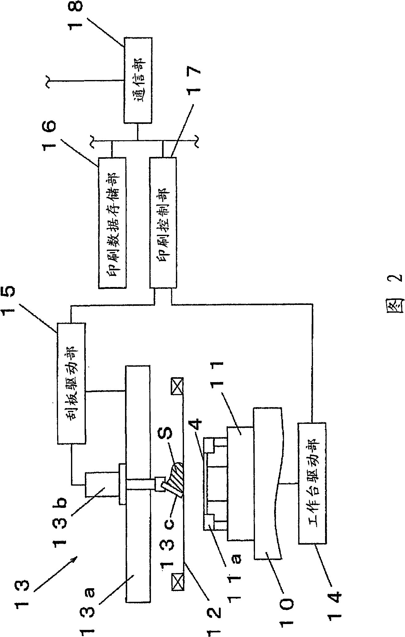
Electronic component mounting system and electronic component mounting method Technical field The present invention relates to an electronic component mounting system and an electronic component mounting method, which mounts electronic components on a plurality of individual substrates held in a carrier by soldering, thereby manufacturing a single-chip mounting board. Background technique An electronic component mounting system is formed by connecting multiple devices for mounting electronic components, such as a solder printing device, an electronic component mounting device, and a reflow device. The electronic component mounting system mounts electronic components on a substrate by soldering to manufacture and mount board. In order to perform high-reliability quality control in such an electronic component mounting system, a technique is known which provides a function of automatically judging whether the component mounting operation has been performed correctly by providing a...
Claims
Login to View More Application Information
Patent Timeline
 Patent Type & AuthorityApplications(China)
IPC IPC(8): H01L21/60H01L21/66H01L21/68H05K3/34H05K13/04
CPCH05K2203/0545H01L24/83H01L24/81H01L2224/81801H05K2201/09918H01L2224/83801H01L2223/54426H01L2224/81121H05K3/1216H05K3/3484H01L23/544H01L2224/83121H05K1/0269H05K3/0097H05K2203/0165H05K2203/166H05K3/303H01L2924/01068H01L2223/54473H05K3/3485Y10T29/49131Y10T29/49144Y10T29/49179Y10T29/53174Y10T29/53178Y10T29/53191Y02P70/50H01L2924/3512H01L2924/00
Inventor井上雅文菊次郁男木原正宏
OwnerPANASONIC CORP