
Printed circuit board

A technology for printed circuit boards and signal pads, which is applied to printed circuit components, electrical connection printed components, and measuring device casings. It can solve problems such as inability to support higher frequency transmission signal tests, and achieve the goal of reducing amplitude attenuation. Effect

Inactive Publication Date: 2010-10-27
HUAWEI TECH CO LTD
View PDF3 Cites 0 Cited by
  • Summary
  • Abstract
  • Description
  • Claims
  • Application Information

AI Technical Summary

Problems solved by technology

Therefore, the use range of the TRL calibration fixture made by using the SMA outlet in the prior art is limited to the transmission signal frequency within 9.5GHz, and cannot support the test of higher frequency transmission signals

Method used


Image

  • Printed circuit board
  • Printed circuit board
  • Printed circuit board

Examples


Embodiment Construction

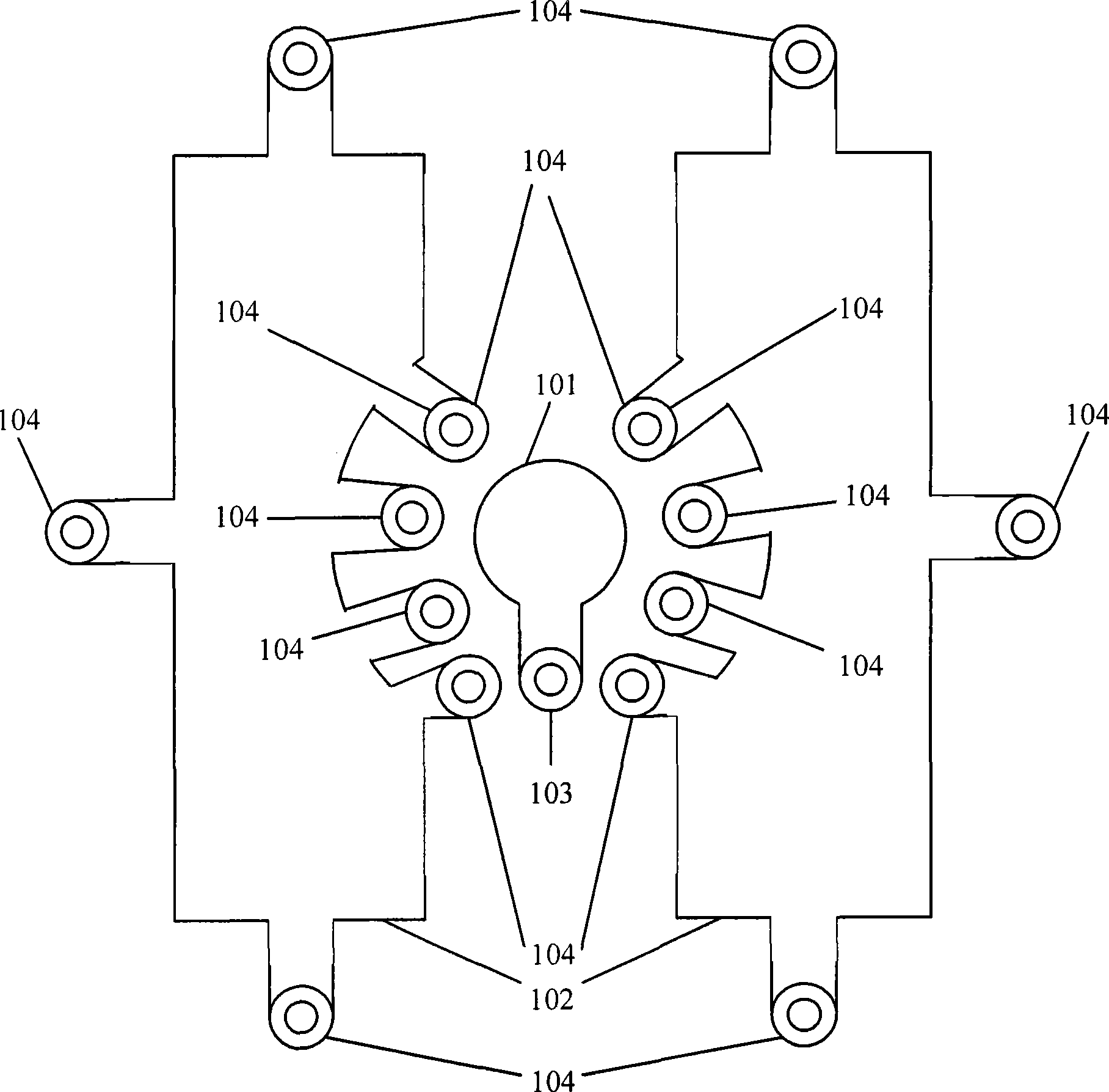
[0016] In the embodiment of the present invention, one end of the coaxial connector is connected to the coaxial cable, and the other end is soldered to the PCB. The signal pad on the PCB is connected to the signal pin of the coaxial connector, and the ground pads on both sides are connected to the ground shell of the coaxial connector.

[0017] The following will clearly and completely describe the technical solutions in the embodiments of the present invention with reference to the accompanying drawings in the embodiments of the present invention. Obviously, the described embodiments are some of the embodiments of the present invention, but not all of them. Based on the embodiments of the present invention, all other embodiments obtained by persons of ordinary skill in the art without creative efforts fall within the protection scope of the present invention.

[0018] Such as figure 1 As shown, it is a schematic diagram of a PCB structure in an embodiment of the present inve...


PUM


Abstract

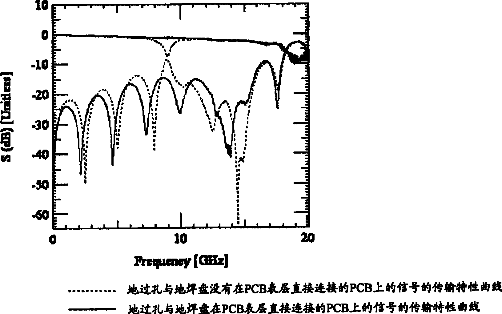
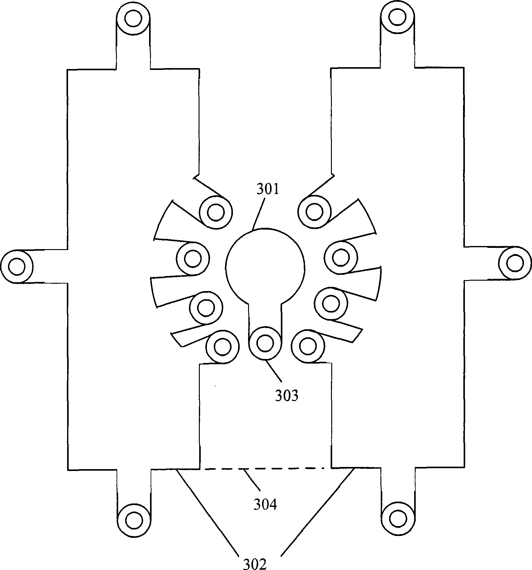
The embodiment of the invention discloses a printed circuit board, which comprises a signal pad, a ground pad, signal through holes and ground through holes; wherein, a circle of ground through holes are distributed around the signal pad; the ground through holes are positioned between the signal pad and the ground pad; the signal through holes are arranged between the ground pad and the signal pad; the distance between the ground through holes and the ground pad is smaller than that between the ground through holes and the signal pad; the distance between the signal through holes and the signal pad is smaller than that between the signal through holes and the ground pad; the ground through holes and the ground pad are directly connected with the surface of the printed circuit board; the signal pad is connected with a signal needle of a coaxial connector; the ground pad is connected with a ground shell of the coaxial connector. The printed circuit board adopts an improved PCB structure and reduces the amplitude attenuation of high-frequency transmission signals.

Description

technical field [0001] The invention relates to the technical field of high-speed design and testing, in particular to a printed circuit board. Background technique [0002] The coaxial connector is a commonly used signal lead-out device in PCB (Printed Circuit Board, printed circuit board) testing. Signal test or connect to other signal ports. In the case of low-speed signal transmission, the impact of the transmission link including the coaxial connector on the signal is very small and can be ignored; as the signal transmission rate increases, the performance of the transmission link has an increasing impact on the signal , mainly manifested in the attenuation of signal amplitude and the increase of jitter. The internal reason that affects the signal quality is whether the characteristic impedance of the transmission link is continuous or not. The signal line of the PCB and the coaxial connector itself is relatively easy to carry out impedance control, while the transmis...

Claims


Application Information

Patent Timeline
Patent Type & Authority Patents(China)
IPC IPC(8): H05K1/11G01R1/04
Inventor 侯维萍
Owner HUAWEI TECH CO LTD
Learn More