LED unit and LED apparatus

An LED device and the same technology, applied in the direction of lighting device, lighting device components, circuit layout, etc., can solve the problems such as difficulty in making LED devices into transparent products, unsightly viewing surface, and increased PCB board area.

Inactive Publication Date: 2009-02-18
BEIJING ZHONGQING MICRO ELECTRIC TECH
View PDF0 Cites 16 Cited by
  • Summary
  • Abstract
  • Description
  • Claims
  • Application Information

AI Technical Summary

Problems solved by technology

Since other electronic circuits and electronic components need to be printed or installed on the conductive pattern layer, they need to occupy a certain horizontal area, and the area of ​​the PCB board needs to be increased accordingly, and the viewing surface of the product is not beautiful; the formed LED device , under a certain lateral area and a certain number of LED units, it is difficult for LED devices to be made into transparent products

Method used


Image

  • LED unit and LED apparatus
  • LED unit and LED apparatus
  • LED unit and LED apparatus

Examples


Embodiment 1

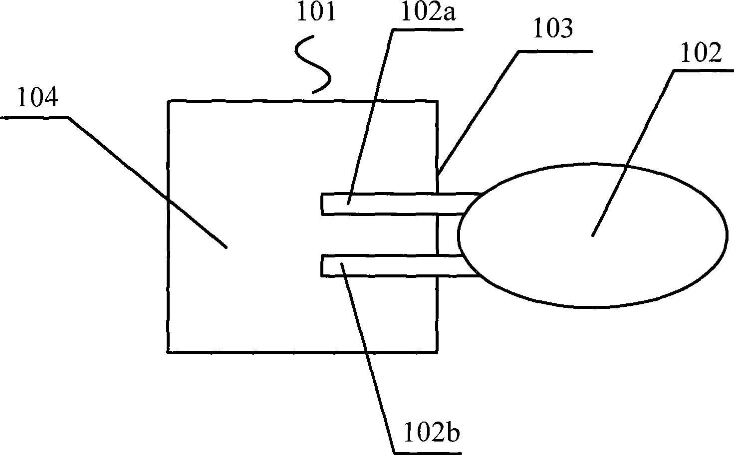
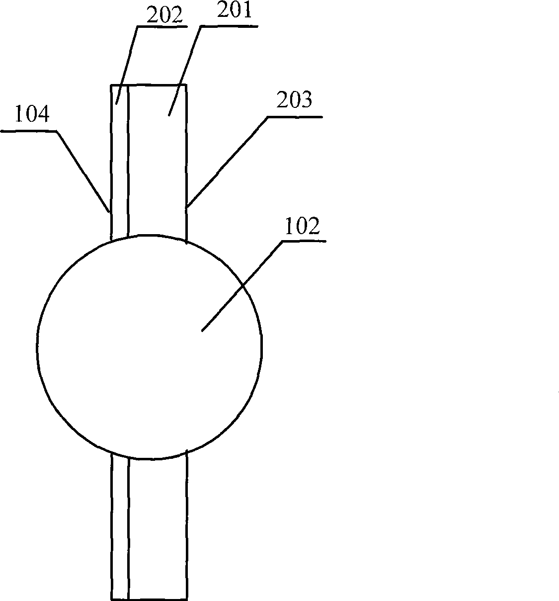
[0028] Such as figure 1 and figure 2 As shown, the LED unit of the present invention includes a PCB board 101 and an LED light emitting diode 102 . The PCB board 101 includes an insulating substrate 201 and a conductive pattern layer 202. The PCB board 101 has at least two sides, the first side 104 and the second side 203; It is arranged on the side 103 of the PCB board. Generally, each PCB board has four sides. Since there is generally only one side for viewing, the light-emitting surface of each LED light-emitting diode should be arranged on the same side, for example, on the side 103 of the PCB board; The present invention does not impose any limitation on the two sides, three sides, or four sides of the PCB respectively.

[0029] In the present invention, the light-emitting surface of the LED light-emitting diode includes each light-transmitting surface of a certain LED light-emitting diode except the base; at the same time, it is better to make the main light-emitting...

Embodiment 2

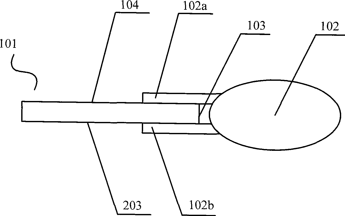
[0033] Such as image 3As shown, the LED unit of the present invention includes a PCB board 101 and an LED light emitting diode 102 . The PCB board 101 has at least two sides, the first side 104 and the second side 203; in order to make the lateral footprint of the LED unit relatively small, the light emitting surface of the LED light emitting diode 102 is arranged on the side 103 of the PCB board, and the LED emits light The diode 102 is arranged on the side 103 of the PCB. The LED light-emitting diode 102 includes a positive pin 102a and a negative pin 102b, the positive pins 102a are respectively arranged on an edge of the side 103 of the PCB, and adjacent to the edge is the first side 104 of the PCB The negative pole pins 102b are respectively arranged on the other edge of the side 103 of the PCB board, and the second side 203 of the PCB board is adjacent to this edge; the positive pole pins 102a are embedded in the first side 104 of the PCB board , and, the cathode pin ...

Embodiment 3

[0038] Such as Figure 4 As shown, the LED unit of the present invention includes a PCB board 101 and an LED light emitting diode 102 . The PCB board 101 has at least two sides, the first side 104 and the second side 203; in order to make the lateral footprint of the LED unit relatively small, the light-emitting surface of the LED light-emitting diode 102 is arranged on the side 103 of the PCB; and, the LED emits light The diode 102 is arranged on the side 103 of the PCB. The LED light-emitting diode 102 includes a positive pole pin 102a and a negative pole pin 102b, and the positive pole pin 102a and the negative pole pin 102b are respectively embedded in the side 103 of the PCB board, so as to achieve the fixed connection between the LED light-emitting diode 102 and the PCB board 101, And at the same time, the LED light emitting diode 102 is arranged on the side 103 of the PCB. In order to ensure the normal operation of the LED light-emitting diode 102 , both the positive ...


PUM


Abstract

The invention discloses a LED unit and a LED device; the LED unit comprises a PCB board and at least a LED; the PCB board comprises an insulated substrate and a conductive pattern printed on the insulated substrate; the light emitting surface of the LED is arranged on the lateral side of the PCB board; the LED is arranged on the lateral side of the PCB board; the LED device is composed of at least two LED units which are integrally connected with each other through connecting units or the PCB boards in the two LED units. The LED unit has the effects of small transverse area occupation, beautiful viewing surface and diverse mounting modes of the LED pins; the LED device composed of the LED units can be manufactured into a transparent product and have strong practicality.

Description

technical field [0001] The present invention relates to an LED illuminating device, in particular to an LED unit and an LED device composed of the LED unit. Background technique [0002] In the LED industry, LED products, such as LED displays, are composed of several LED pixels connected to each other. Each LED pixel can be used as an LED unit, including at least one LED light-emitting diode and a PCB board for installing the LED light-emitting diode. . In a traditional LED unit, LED light-emitting diodes and other electronic circuits and electronic components are installed and arranged on the conductive pattern layer on the front of the PCB. Since other electronic circuits and electronic components need to be printed or installed on the conductive pattern layer, they need to occupy a certain lateral area, and the area of ​​the PCB board needs to increase accordingly, and the viewing surface of the product is not beautiful; the formed LED device , under a certain lateral a...

Claims


Application Information

Patent Timeline
Patent Type & Authority Applications(China)
IPC IPC(8): F21V19/00F21V23/00F21Y101/02F21Y115/10
Inventor 商松
Owner BEIJING ZHONGQING MICRO ELECTRIC TECH
Why Eureka
Try Eureka