Zoom optic lens

A technology of optical zoom and lens, applied in the field of optical zoom lens, can solve problems such as difficult to meet high resolution and large resolution

Inactive Publication Date: 2009-03-18
HONG FU JIN PRECISION IND (SHENZHEN) CO LTD +1
View PDF0 Cites 17 Cited by
  • Summary
  • Abstract
  • Description
  • Claims
  • Application Information

AI Technical Summary

Problems solved by technology

In the electronic zoom mode, the greater the magnification of the image, the greater the resolution, which is difficult to meet the requirements of high resolution

Method used


Image

  • Zoom optic lens
  • Zoom optic lens
  • Zoom optic lens

Examples


Embodiment 1

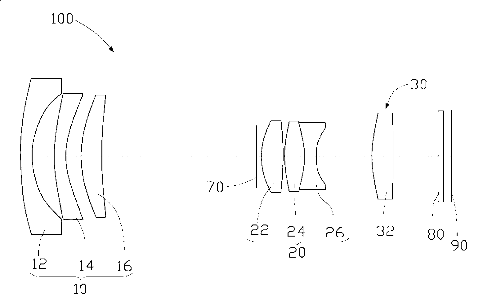
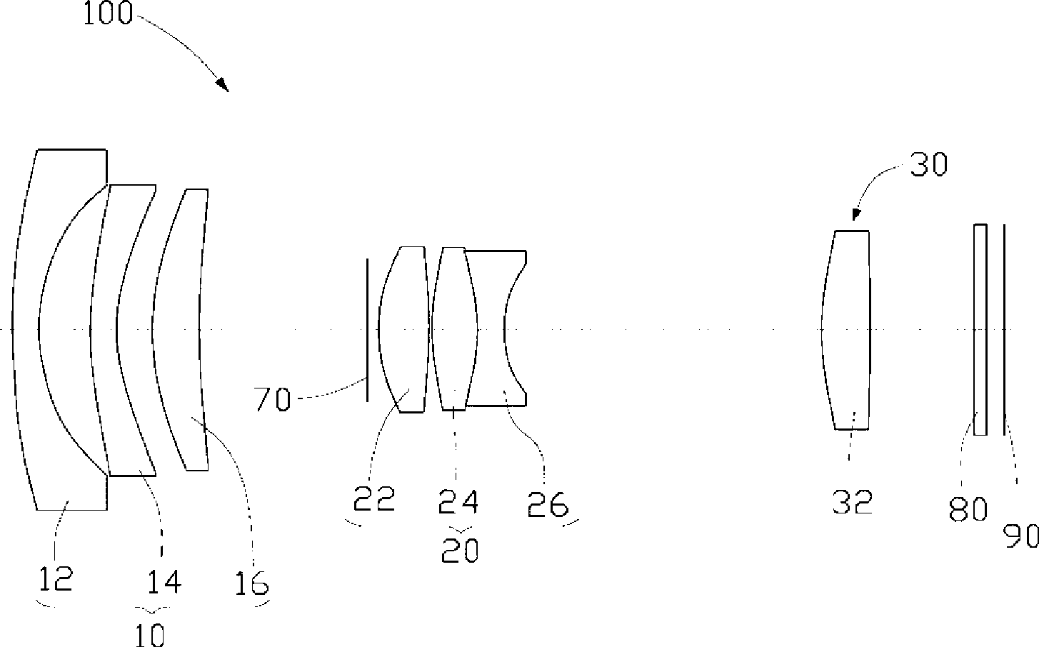
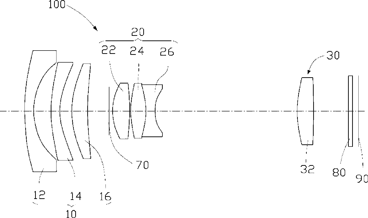
[0049] Each optical element of the optical zoom lens 100 satisfies the conditions in Table 1 to Table 3, and its f=6.27~17.9mm; F W =6.27mm; F No =2.9~4.9; 2ω=59°~22°.

[0050] Table 1

[0051] surface Radius of curvature (mm) Thickness (mm) Refractive index Abbe number

[0052] The surface of the first lens 12 on the object side 24.41 1 1.69 48.5 The image-side surface of the first lens 12 6.5 1.76 --- --- The second lens 14 is on the object side surface 11.16 1 1.531 56.04 The surface of the second lens 14 on the image side 5.41 1.23 --- --- The surface of the third lens 16 on the object side 8.25 1.86 1.6 26.64 The surface of the third lens 16 on the image side 29.64 D6 (variable) --- --- Aperture surface gigantic 0.3 --- --- The fourth lens 22 is on the object side surface 5.45 1.909 1.531 56.04 The surface of the fourth lens 22 on the image side -16.27 0.1 --- --...

Embodiment 2

[0060] Each optical element of the optical zoom lens 100 meets the conditions of Table 4~Table 6, and its f=6.85~19.6mm; F W =6.85mm; F No =2.9~4.9; 2ω=59°~22°.

[0061] Table 4

[0062] surface Radius of curvature (mm) Thickness (mm) Refractive index Abbe number The surface of the first lens 12 on the object side 23.59 1 1.69 48.5 The image-side surface of the first lens 12 6.23 1.87 --- --- The second lens 14 is on the object side surface 8.99 1 1.531 56.04 The surface of the second lens 14 on the image side 5.58 1.09 --- --- The surface of the third lens 16 on the object side 8.86 1.84 1.6 26.64 The surface of the third lens 16 on the image side 28.84 D6 (variable) --- --- Aperture surface gigantic 0.3 --- ---

[0063] The fourth lens 22 is on the object side surface 5.76 2.03 1.531 56.04 The surface of the fourth lens 22 on the image side -18.1 0.1 --- --- Th...


PUM


Abstract

An optical zoom lens comprises a first lens group of negative optical power, a second lens group of positive optical power and a third lens group of positive optical powder, from the object side to the image side. The optical zoom lens meets following conditions: -0.45<FW / f1<-0.3 and 0.4<f2 / f1<0.8, wherein FW is the minimum effective focus of the optical zoom lens, f1 is the focus of the first lens group and f2 is the focus of the second lens group.

Description

technical field [0001] The invention relates to an optical zoom lens, in particular to an optical zoom lens for electronic equipment. Background technique [0002] In recent years, with the development of multimedia, there is an increasing demand for imaging elements of solid-state imaging devices such as CCD (Charged Coupled Device) or CMOS (Complementary Metal Oxide Semiconductor) used in laptop computers, videophones, and mobile phones. With the development of miniaturization and higher pixel count, high contrast is required for the camera body and the lens mounted on it, and further miniaturization is also required. [0003] On the other hand, due to the improvement of the process technology of these solid-state imaging devices such as CCD or CMOS, imaging devices with each pixel only a few microns in size have been produced, which makes the system miniaturized and improves the resolution requirements of the camera lens. In the electronic equipment using the imaging ele...

Claims


Application Information

Patent Timeline
Patent Type & Authority Applications(China)
IPC IPC(8): G02B15/16G02B9/12G02B13/18
CPCG02B15/177G02B15/143507
Inventor 许德伦黄俊翔
Owner HONG FU JIN PRECISION IND (SHENZHEN) CO LTD
Why Eureka
Try Eureka