Method for manufacturing double-stress membrane complementary metal oxide semiconductor (CMOS) transistor

A technology of oxide semiconductors and complementary metals, which is applied in semiconductor/solid-state device manufacturing, electrical components, circuits, etc., can solve the problems of the stability of complementary metal oxide semiconductor transistors, affecting the process, etc., so as to improve stability and increase The effect of the process window

CN101447457AInactive Publication Date: 2009-06-03SEMICON MFG INT (SHANGHAI) CORP
1 Cites 20 Cited by

Patent Information

Authority / Receiving Office
CN · China
Current Assignee / Owner
Publication Date
2009-06-03
Estimated Expiration
Not applicable · inactive patent

Smart Images

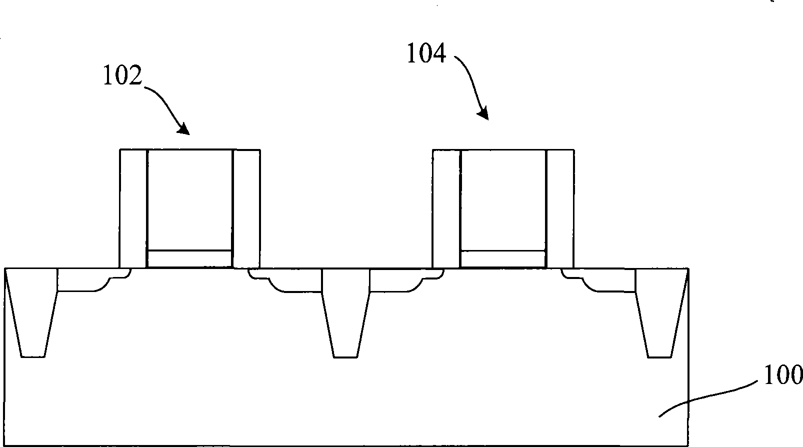
  • Figure 1
    Figure 1
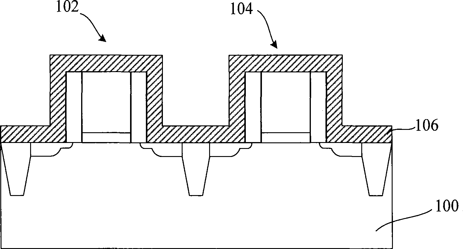
  • Figure 2
    Figure 2
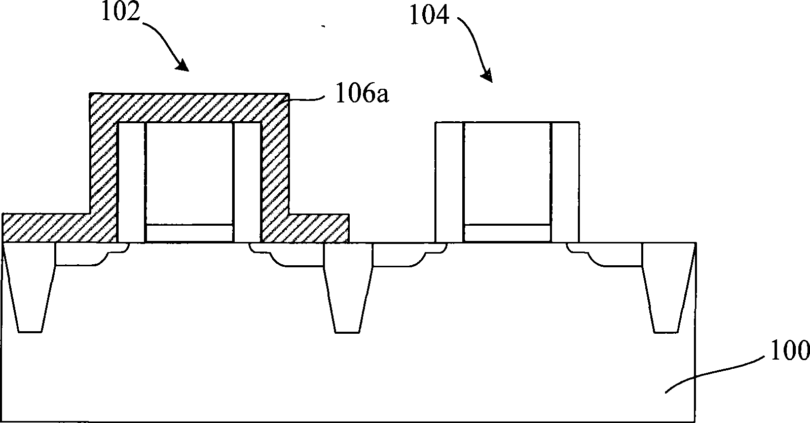
  • Figure 3
    Figure 3
Patent Text Reader

Abstract

The invention discloses a method for manufacturing a double-stress membrane CMOS, comprising: a semiconductor substrate which comprises a first transistor and a second transistor is provided; a doped first stress membrane is formed on the first transistor; a second stress membrane is formed on the first stress membrane and the second transistor, wherein, the thickness of the second stress membrane is at least equal to the sum of the thicknesses of a grid medium layer, a grid and the first stress membrane of the first transistor; the second stress membrane is flattened, so that the surface of the first stress membrane is exposed out; photoresist patterns are formed on the exposed surface of the first stress membrane and the second stress membrane above a grid of the second transistor, wherein, the line width of the photoresist patterns above the grid of the second transistor and on the second stress membrane is larger than the line width of the grid of the second transistor; the second stress membrane which is not covered by the photoresist patterns is etched until the second stress membrane on the first stress membrane is removed. No bossed defects can be produced at the joint of a tension stress membrane and a compressive stress membrane layer.
Need to check novelty before this filing date? Find Prior Art

Description

technical field

[0001] The invention relates to the technical field of semiconductor manufacturing, in particular to a manufacturing method of a double stress film complementary metal oxide semiconductor transistor (CMOS). Background technique

[0002] With the continuous development of semiconductor manufacturing technology, the size of metal-oxide-semiconductor transistors is also decreasing day by day, but there are higher requirements for their physical properties such as reliability and response rate.

[0003] The important factor affecting the response rate in metal oxide semiconductor transistors is the carrier mobility. Under the same driving voltage, the transistor with large carrier mobility has a faster response rate. People always use various methods to To improve the carrier mobility of metal-oxide-semiconductor transistors to obtain higher response rates. At present, the industry has developed a "strained silicon technology" to improve the mobility of carriers...

Examples

Embodiment Construction

[0054] The specific embodiments of the present invention will be described in detail below in conjunction with the accompanying drawings.

[0055]Covering the stress film on the MOS transistor can increase the mobility of carriers in the conduction channel, thereby improving the response rate of the MOS device. The NMOS transistor in the CMOS is covered with a tensile stress film, and the PMOS transistor is covered with a compressive stress film, which can improve the carrier mobility of electrons and holes in the NMOS and PMOS transistors, respectively.

[0056] In an embodiment of the present invention, a method for manufacturing a dual stress film complementary metal oxide semiconductor transistor is provided;

[0057] Firstly, a first stress film for improving carrier mobility of the first transistor is formed on the first transistor, and then a first stress film for improving carrier mobility of the second transistor is formed on the first stress film and the second trans...