

Method of manufacturing a semiconductor device and molding die
a semiconductor device and molding die technology, applied in the direction of dough shaping, manufacturing tools, applications, etc., can solve the problems of insufficient adhesion the heat generated on the semiconductor chip cannot be sufficiently distributed and discharged, and the joining pressure between the heat spreader and the molding resin is generally not high, so as to achieve favorable diffusion and discharge of heat generated on the semiconductor chip. , the effect of high thermal conductivity
- Summary
- Abstract
- Description
- Claims
- Application Information
AI Technical Summary
Benefits of technology
Problems solved by technology
Method used
Image

Examples
first embodiment
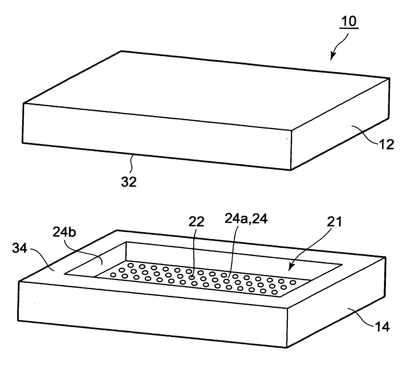
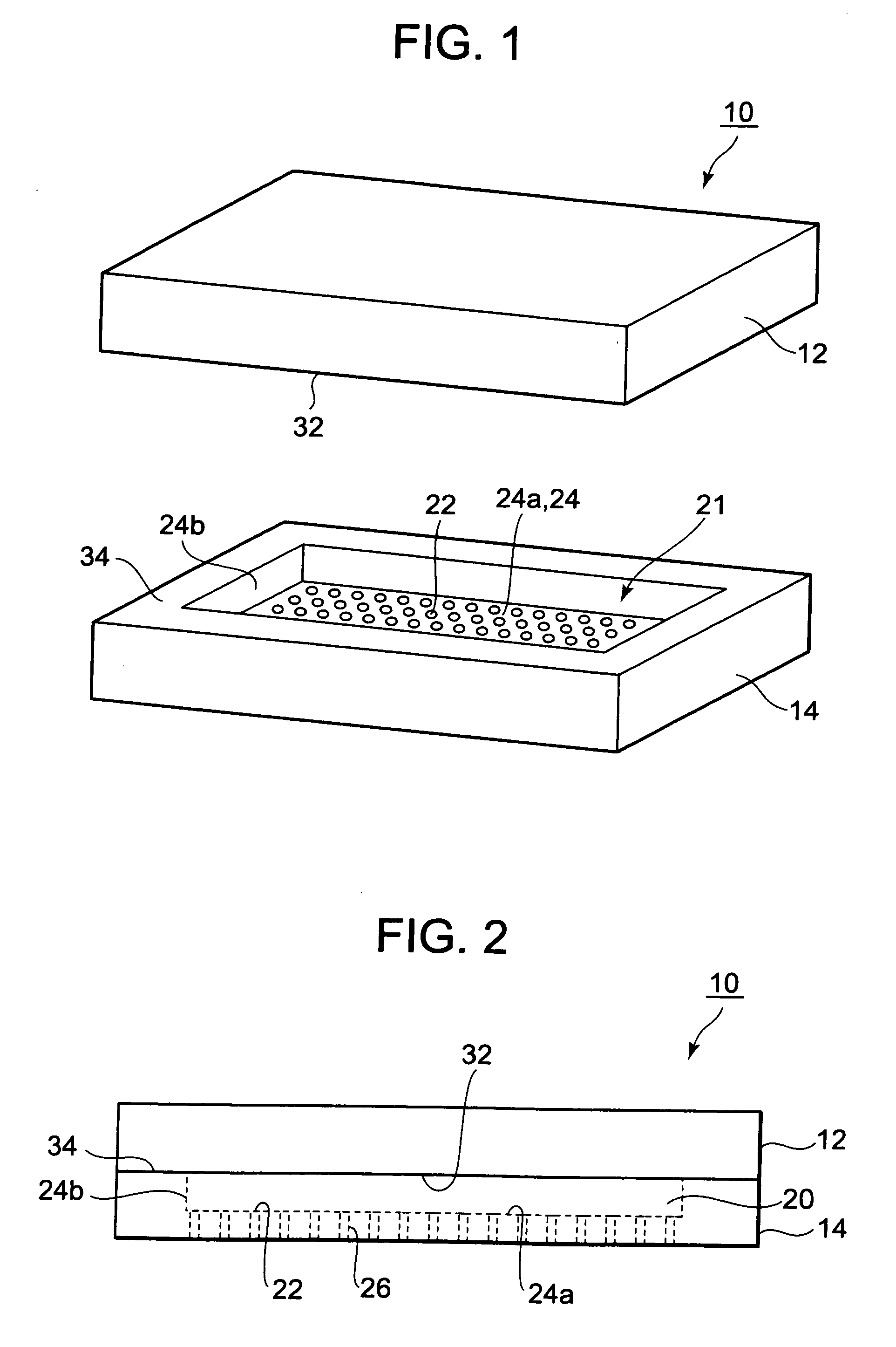
[0026]FIG. 1 is a perspective view showing an example of a molding die 10 according to the present embodiment. The molding die 10 is used by combining a second molding die 12 and a first molding die 14. FIG. 2 is a lateral view of the molding die 10 joining the second molding die 12 and the first molding die 14.
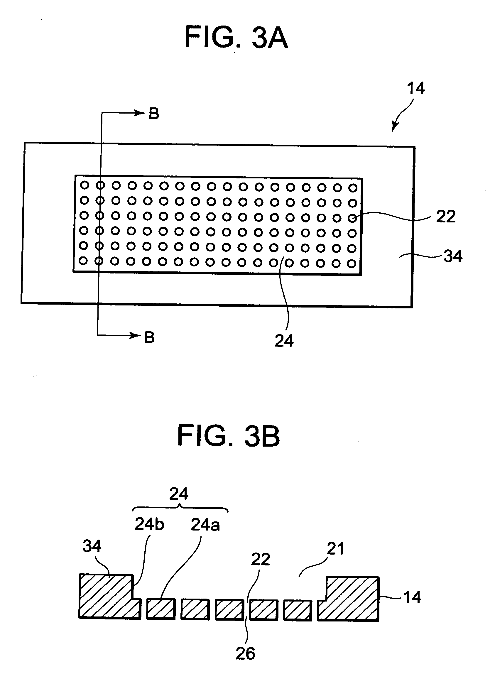
[0027]FIG. 3A is a plan view of the first molding die 14 according to the present embodiment, while FIG. 3B is a B-B cross sectional view thereof.
[0028]FIG. 4A is a lateral view of a substrate 54 on which semiconductor chips 50 seal-molded by the molding die 10 according to the present embodiment are mounted, while FIG. 4B is a plan view (bottom view) thereof.
[0029]First, an overview of the molding die 10 according to the present embodiment will be given.
[0030]The molding die 10 includes: the second molding die 12 on which the substrate 54 mounted with the semiconductor chips 50 is set; and the first molding die 14 that forms a cavity 20 when combined with the second molding ...
second embodiment
[0119]FIG. 7A is a plan view of a first molding die 14 according to the present embodiment, while FIG. 7B is a B-B cross sectional view thereof.
[0120]In the first molding die 14 according to the present embodiment, apertures 22 are provided with tapers 28 whose diameter increases towards a cavity 20 (a cavity recess 21). Accordingly, since a heat spreader 60 bulges and deforms along the tapers 28 during pressing, initial deformation of the heat spreader 60 is facilitated. In addition, as bulging and deformation of the heat spreader 60 commence during pressing, bulging is suppressed in a small-diameter section of vents 26 which are a deep section of the tapers 28. As a result, excessive bulging and breakage of the heat spreader 60 at the apertures 22 can be prevented.
[0121]Furthermore, a part of the apertures 22 do not communicate with the outside of the first molding die 14 and form aperture ends of depressions 29 that are blind holes. Accordingly, by adsorbing and holding the heat ...
PUM
| Property | Measurement | Unit |
|---|---|---|
| Force | aaaaa | aaaaa |
| Pressure | aaaaa | aaaaa |
| Diameter | aaaaa | aaaaa |
Abstract
Description
Claims
Application Information