Multi-Layered Product for Printed Circuit Boards, and a Process for Continuous Manufacture of Same

a technology of printed circuit boards and products, applied in the direction of magnetic recording, lamination, electrical equipment, etc., can solve the problems of low efficiency, circuitry is prone to loss, and part of transmitted energy is lost, and achieves the effect of reducing production costs and reducing production costs

Inactive Publication Date: 2009-04-30
OSTROVSKY VALERY
View PDF7 Cites 3 Cited by
  • Summary
  • Abstract
  • Description
  • Claims
  • Application Information

AI Technical Summary

Benefits of technology

[0015]The present invention discloses a product for use in manufacturing a printed circuit board, having a novel dielectric material, which grants it advantages over prior art PCB laminates. There is additionally disclosed a novel method of manufacture of the product, that allows polypropylene coating and lamination of metal foil, for production of PCBs for microwave circuitry. The resultant novel product is resistant to peeling and has greater energy efficiency during use, than prior art PCBs.

Problems solved by technology

When electric currents of 1-80 GHz are propagated through transmission lines on such a printed circuit board (PCB hereinafter), part of the transmitted energy is lost due to dielectric losses in the surrounding material.
If not, the circuitry will be prone to losses and the efficiency will be low.
Each of these dielectric materials suffers from a specific drawback, making each less than ideal.
In circuit boards having glass-impregnated plastics such as the polyester-glass material as the dielectric substrate, the concentration of polar pieces of the resin molecules and glass fiber resonate at high microwave frequencies cause considerable dissipation of energy.
However they are expensive for a number of reasons.
Teflon™ is itself expensive.
The manufacturing involves a cyclic lamination process using hot presses; the yield of this process is low and Teflon™ is not ideal due to its polarity.
Polyester also has a significant dissipation factor (DF) fluctuation over temperatures within the range of 25° C. to 80° C. and this limits its applications.
This means that it cannot be used in standard assembly processes.
When gluing polyethylene laminations, the high temperatures required for setting the glue can give rise to local softening of the polyethylene and cause it to creep, resulting in variations in the thickness of the dielectric material.
A further disadvantage of polyethylene is that heat absorbed by the polyethylene substrate when laminated with molten bonding materials causes high-tension strain between the foil and the plastic as a result of the existence of different thermal contraction rates of the various layers.
This results in warping in those areas where the remaining copper (namely that which remains after etching) has the strength to resist shrinkage.
However, application of polypropylene to metal foil PCBs is not obvious, since when no adhesive is used, and molten polypropylene is poured or otherwise applied onto PCBs, it will easily peel off upon cooling.

Method used


Image

  • Multi-Layered Product for Printed Circuit Boards, and a Process for Continuous Manufacture of Same
  • Multi-Layered Product for Printed Circuit Boards, and a Process for Continuous Manufacture of Same
  • Multi-Layered Product for Printed Circuit Boards, and a Process for Continuous Manufacture of Same

Examples


Embodiment Construction

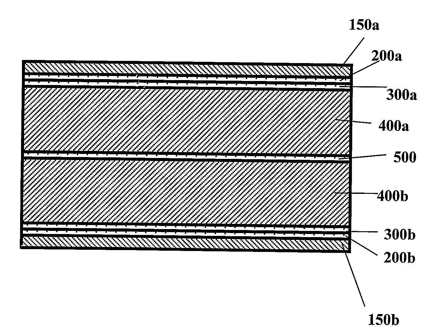
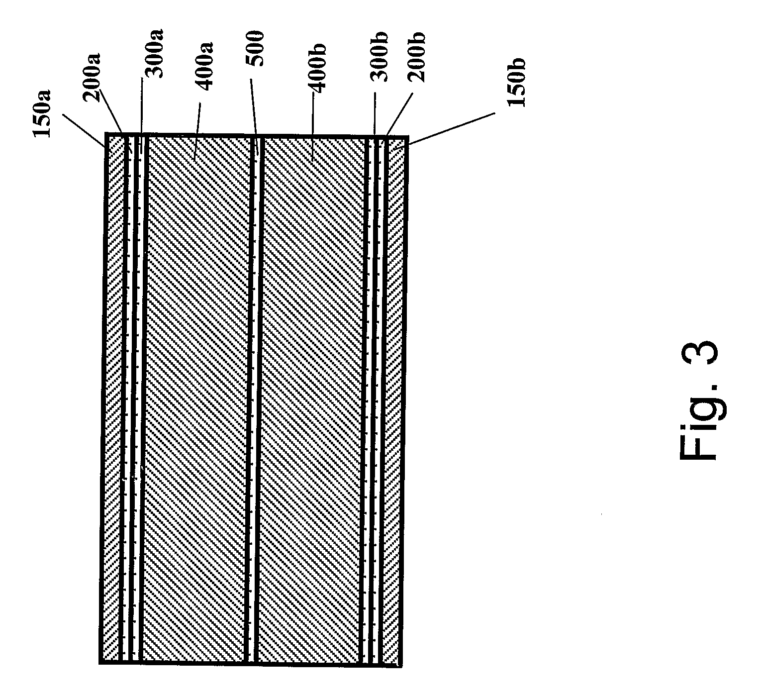
[0032]It is important to note that the process of the invention is a continuous process, allowing circuit boards to be produced on an automated production line in a roll-to-roll manner. The speed of the continuous process is relatively high, and thus cost efficient compared to prior art processes, and the process allows production of 50-150 meters of multi-layered product for each minute of operation of the production process.

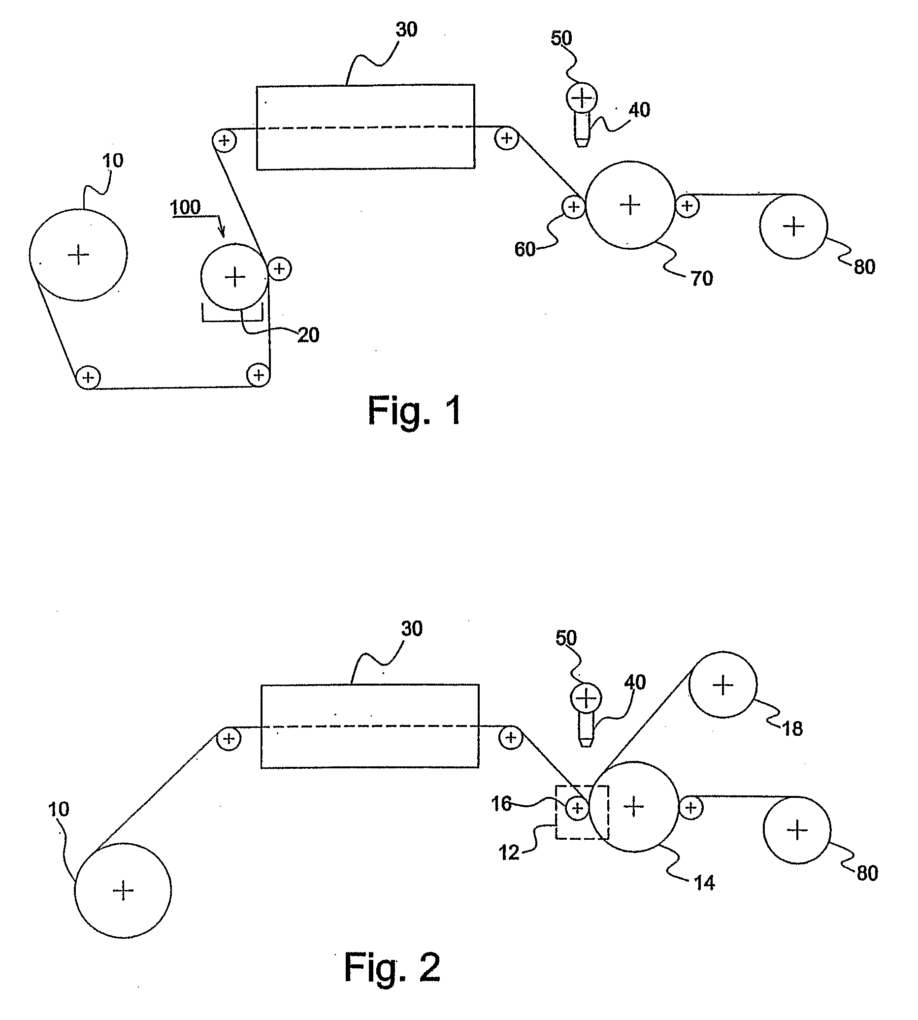
[0033]FIG. 1 illustrates the first segment of the production line used to produce the multi-layered product. Referring to FIG. 1, conductive metal foil, for instance electrodeposited copper foil, is unwound in an unwinding station (10). Preferably, as a first step in the process of the invention, the conductive metal foil is primed at a priming station (100), to increase its adhesive properties. The conductive foil is primed with a material such as R-1559 (produced by Mica Corp., Shelton, Conn.) which is an aqueous primer comprising polypropylene (PP) molecules...


PUM

PropertyMeasurementUnit
temperatureaaaaaaaaaa

Abstract

The invention provides a low energy loss, multi-layered polypropylene/metal foil product useful for further processing into printed circuit boards and antenna boards for microwave circuitry. A continuous process for manufacture of the product is described. The process comprises the steps of: providing metal foil; optionally, extrusion coating molten polypropylene upon said metal foil, to obtain a foil coated with a polypropylene foundation layer; casting a molten polypropylene tie-layer upon said metal foil or upon said coated metal foil; and laminating a polypropylene sheet on said tie layer. In the process, heat is applied to induce fusing of the layers of the multi-layered product.

Description

FIELD OF THE INVENTION[0001]The present invention relates to a multi-layered product useful for manufacturing printed circuit boards and antenna boards for microwave circuitry, having low losses of energy, and to a method for producing the same.BACKGROUND OF THE INVENTION[0002]Microwave circuit boards, are typically formed of two conductive metal foils, having a material between them which has a predetermined dielectric constant; this material is hereafter termed the “dielectric substrate”. The board is then etched, or solvent-treated, to remove specific areas of the conductive foil, to create a circuit pattern, whose shape depends on the intended use. U.S. Pat. No. 4,335,180 to Traut describes a microwave circuit board and a method for its production.[0003]When electric currents of 1-80 GHz are propagated through transmission lines on such a printed circuit board (PCB hereinafter), part of the transmitted energy is lost due to dielectric losses in the surrounding material. Thus, th...

Claims


Application Information

Patent Timeline
Patent Type & Authority Applications(United States)
IPC IPC(8): B32B15/085B29C70/88B32B37/00B32B37/02H05K1/05
CPCB32B15/085Y10T428/269B32B27/08B32B27/18B32B27/32B32B37/153B32B2250/40B32B2264/102B32B2311/12B32B2323/10B32B2457/08H05K1/032H05K3/022H05K3/386H05K2201/0158H05K2201/0209H05K2201/0355H05K2201/0358H05K2203/0143H05K2203/0759H05K2203/1545Y10T428/265Y10T428/264B32B15/20Y10T428/31692
Inventor OSTROVSKY, VALERY
Owner OSTROVSKY VALERY
Why Eureka
Try Eureka