

Device for reazliing time delay integral of area array CMOS image sensor
A technology of time-delay integration and image sensor, which is applied in the special application field of CMOS image sensor, can solve the problems that photoelectron transfer and integration cannot be carried out, TDICMOS devices are not easy to obtain, etc., and achieve the effect of flexible selection
- Summary
- Abstract
- Description
- Claims
- Application Information
AI Technical Summary
Problems solved by technology
Method used
Image

Examples
Embodiment Construction
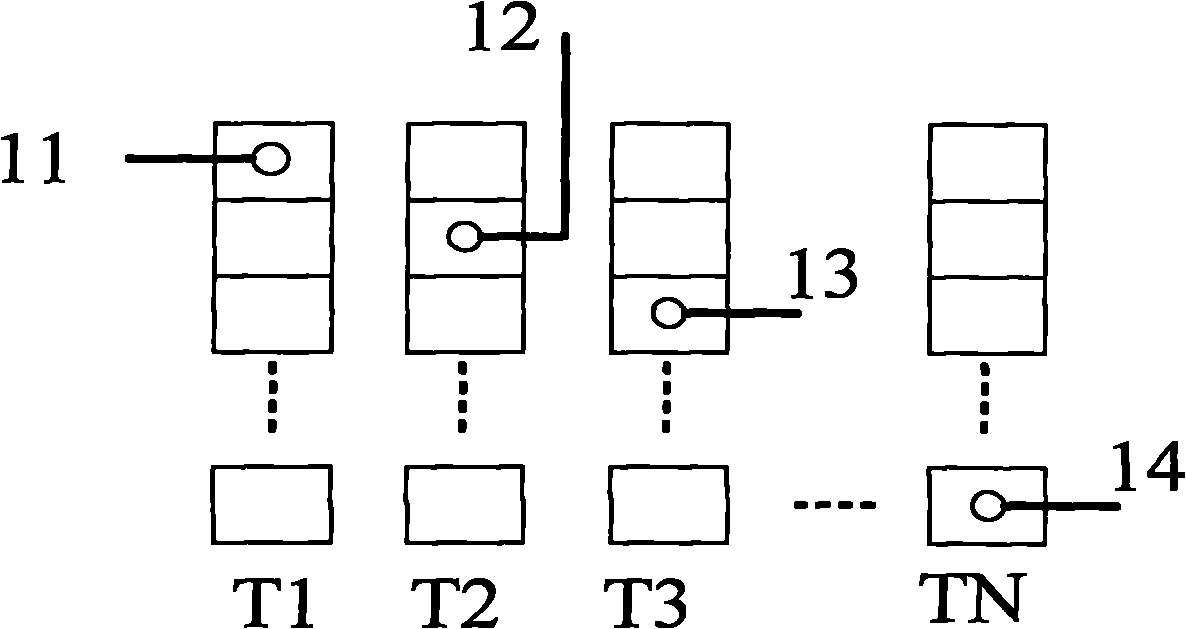
[0023] The principle of TDI CCD time delay integration is as follows: figure 1 shown. At time T1, the first row of pixels 11 is exposed to generate photoelectrons e1; at T2 time, the second row of pixels 12 is exposed to generate photoelectrons e2, and at the same time, the photoelectrons e1 of the first row of pixels are transferred to the second row of pixels 12 and e2 The second-level integration result is obtained by adding; at time T3, the photoelectron e3 generated by the exposure of the pixel 13 in the third row is accumulated with the photoelectron e1 and photoelectron e2 to obtain the third-level integration result. By analogy, if the number of integration stages is N, then the pixels 14 in the Nth row integrate the same target N times to obtain the final N-level integration results, thereby improving the sensitivity of the CCD image sensor.
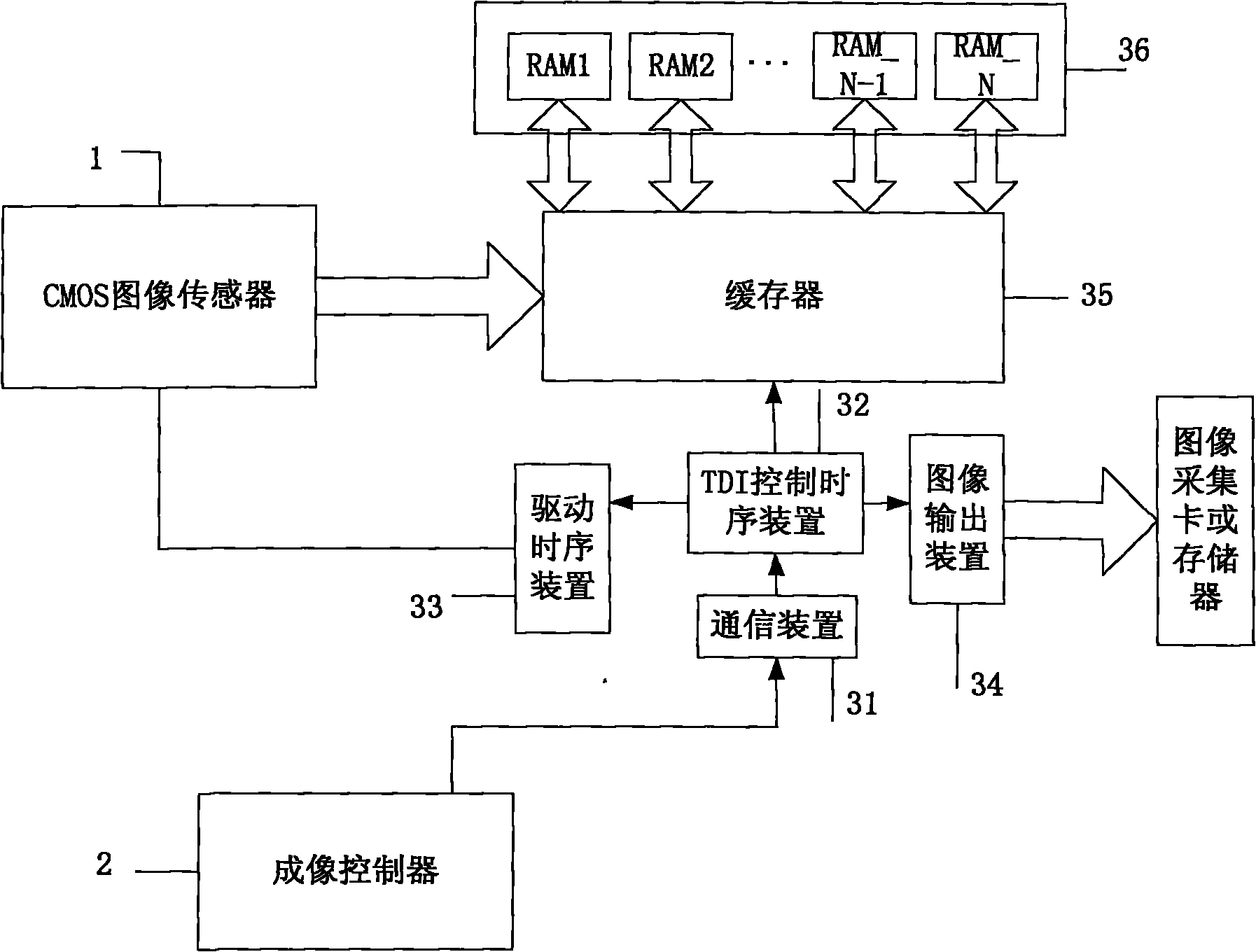
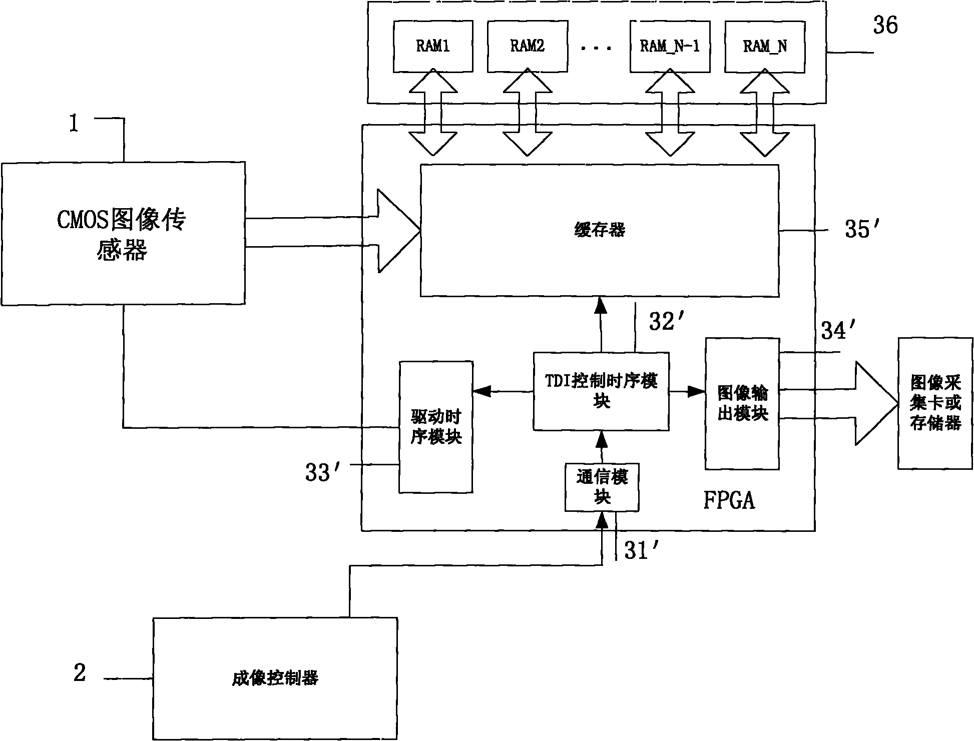
[0024] like figure 2 As shown, the device for realizing the time delay integration of the area array CMOS image sensor of t...
PUM
 Abstract
Description
Claims
Application Information