
Fault testing method for interconnection resource of programmable logic device

A technology of interconnection resources and programming logic, applied in the field of automatic fault traversal testing of interconnection resources of general-purpose programmable logic devices, can solve the problem of high computational complexity and achieve the effect of fewer configurations

Inactive Publication Date: 2010-11-10
FUDAN UNIV
View PDF0 Cites 19 Cited by
  • Summary
  • Abstract
  • Description
  • Claims
  • Application Information

AI Technical Summary

Problems solved by technology

However, for the short-circuit fault of the interconnection segment, using the particularity of the hardware structure of the Virtex chip, all unused interconnection resources can be driven to "0" or "1", which has limitations in the hardware structure. In addition, for each The computational complexity required to map the interconnected resources in each direction is very high

Method used


Image

  • Fault testing method for interconnection resource of programmable logic device
  • Fault testing method for interconnection resource of programmable logic device
  • Fault testing method for interconnection resource of programmable logic device

Examples


Embodiment 1

[0047] Take the FPGA structure model with a 3*3 array scale as an example, the model scale is 3*3, which means that there are 3 CLBs in the horizontal and vertical directions. There are 2 double lines and one long line in the channel, and the generated number of PIPs to be tested is 176. The specific structure of the FPGA chip is described as follows:

[0048]

[0049]

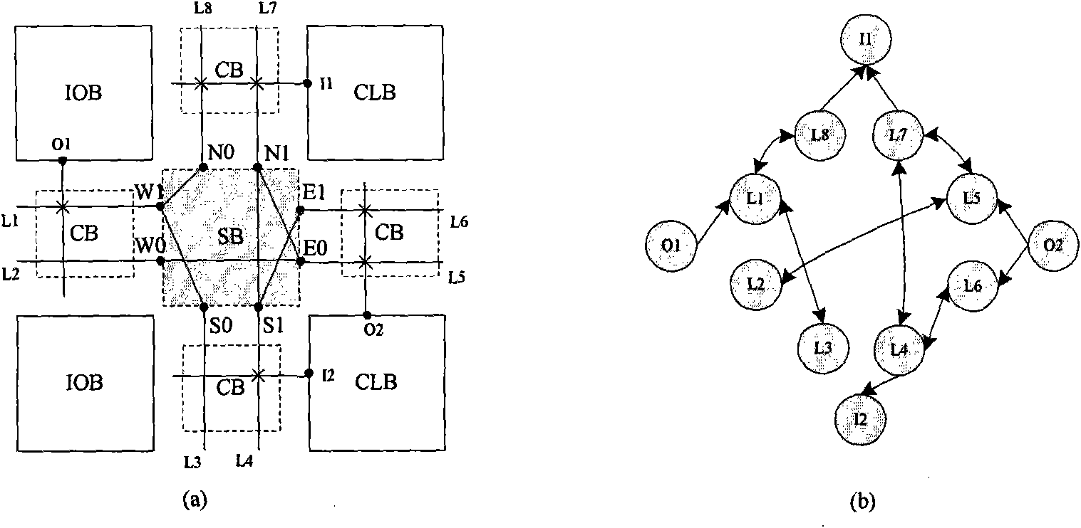
[0050] According to the structure description file, the corresponding wiring resource diagram is generated to generate the test resource. The specific description is as follows:

[0051]

[0052]

[0053] Then select the direction of the line network in turn, set the weight of each side according to the weight formula and sort them. Run the improved Kruskal algorithm to get the bit stream configuration file, the result is as follows Figure 4 shown.

[0054] If the generated configuration file has met the complete conditions of the test, the program stops, otherwise continue to select the line n...


PUM


Abstract

The invention belongs to the technical field of an electron, particularly relates to an automated fault traversal testing method for an interconnection resource of a programmable logic device. The invention provides a method for automatically generating a test configuration set, which is irrelevant to the application; the weights of all sides are set according to the trend of a net by establishing a wiring resource map; and the configuration set is generated automatically by utilizing an improved Kruskal algorithm. For different interconnection structures of FPGA, the method achieves 100% coverage rate for the open circuit and short circuit fault in the interconnection resource, and has a few numbers of testing configurations, fast running speed and no dependency on a specified hardware structure.

Description

technical field [0001] The invention belongs to the field of electronic technology, and in particular relates to an automatic fault traversal test method for interconnection resources of general-purpose programmable logic devices. Background technique [0002] The general-purpose programmable logic device needs to ensure that the programmable logic device (Field Programmable Gate Array FPGA) chip can correctly realize the required circuit function for any user configuration. Usually, due to various user configurations, and with the increase of the FPGA chip scale, the time to configure the FPGA varies from milliseconds to seconds, so it is impossible to download all possible user configurations to the FPGA chip for troubleshooting Walk through the tests. In order to complete the fault traversal test of the FPGA chip, a special configuration set that has nothing to do with the application (Application Independent) must be downloaded to the FPGA chip to detect various faults ...

Claims


Application Information

Patent Timeline
Patent Type & Authority Applications(China)
IPC IPC(8): G01R31/3185G01R31/02
Inventor 王伶俐童家榕陈更生代莉
Owner FUDAN UNIV
Learn More