Thin-film solar cell and process for its manufacture
A solar cell, solar-grade technology, applied in final product manufacturing, sustainable manufacturing/processing, circuits, etc.
- Summary
- Abstract
- Description
- Claims
- Application Information
AI Technical Summary
Problems solved by technology
Method used
Image

Examples
Embodiment Construction
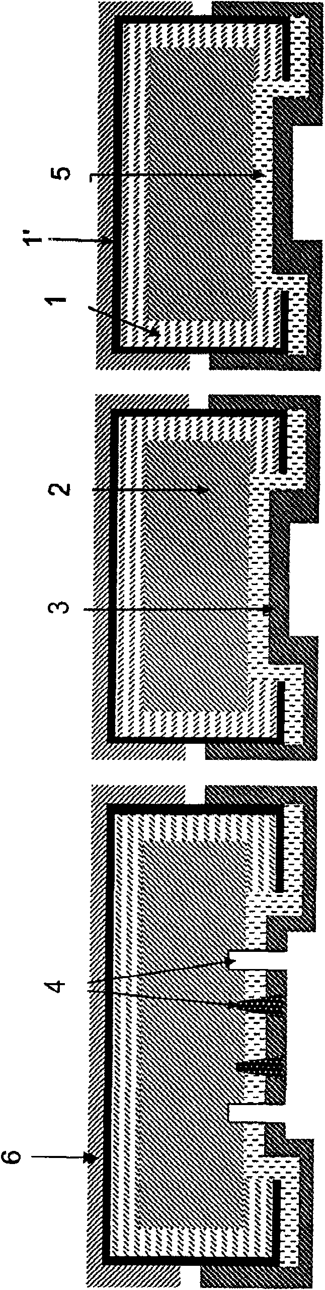
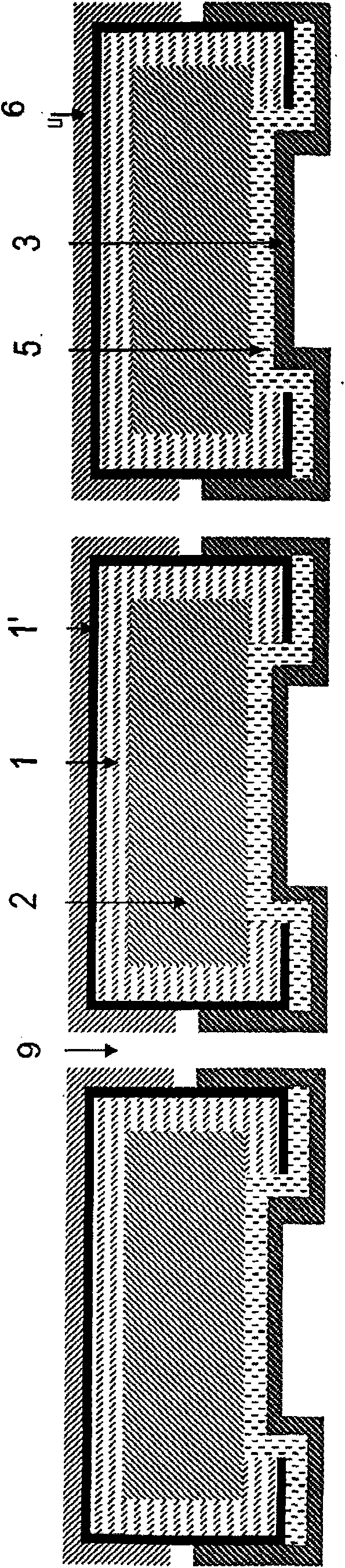
[0033] figure 1 In a cross-sectional view, a first embodiment of the solar cell of the invention is shown.
[0034] The base layer 1 and the emitter layer 1' of the solar cell surround a through hole in the low cost substrate 2. This is achieved by simultaneously depositing said layers of the solar cell on the front surface of the substrate and directly into the vias. The substrate can be highly doped and highly conductive. Thus, the substrate can be used to conduct current laterally to the base contacts, which allows more flexibility in the design of interdigitated contacts. It is also possible to use an insulating substrate, in which case the deposited base should serve to conduct electricity. The rear surface of the substrate can be destroyed without reducing the efficiency of the solar cell, which greatly simplifies the determination of the interdigitated contact pattern. Metal 3 can be deposited over the entire rear surface, and then the base and emitter contact...
PUM
 Abstract
Description
Claims
Application Information
 - R&D
- Intellectual Property
- Life Sciences
- Materials
- Tech Scout
- Unparalleled Data Quality
- Higher Quality Content
- 60% Fewer Hallucinations
Browse by: Latest US Patents, China's latest patents, Technical Efficacy Thesaurus, Application Domain, Technology Topic, Popular Technical Reports.
© 2025 PatSnap. All rights reserved.Legal|Privacy policy|Modern Slavery Act Transparency Statement|Sitemap|About US| Contact US: help@patsnap.com