Check patentability & draft patents in minutes with Patsnap Eureka AI!

Pixel structure

A pixel structure, pixel technology, applied in nonlinear optics, instruments, optics, etc., can solve the problem of pixel static charge accumulation, and achieve the effect of reducing burn-in problems and high-quality display technology

Inactive Publication Date: 2011-05-25
CPT DISPLAY TECH FUJIAN +1
View PDF0 Cites 0 Cited by
  • Summary
  • Abstract
  • Description
  • Claims
  • Application Information

AI Technical Summary

Problems solved by technology

[0005] The technical problem to be solved by the present invention is to provide a pixel structure to solve the problem of traditional pixel electrostatic charge accumulation

Method used


Image

  • Pixel structure
  • Pixel structure
  • Pixel structure

Examples


Embodiment Construction

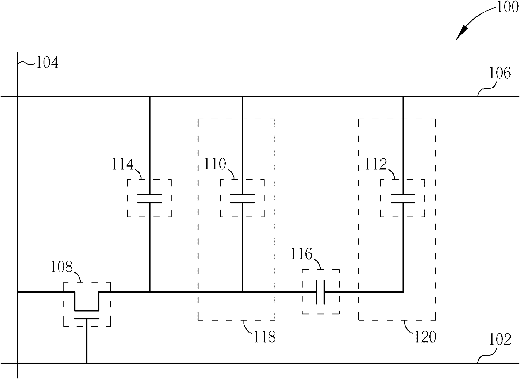
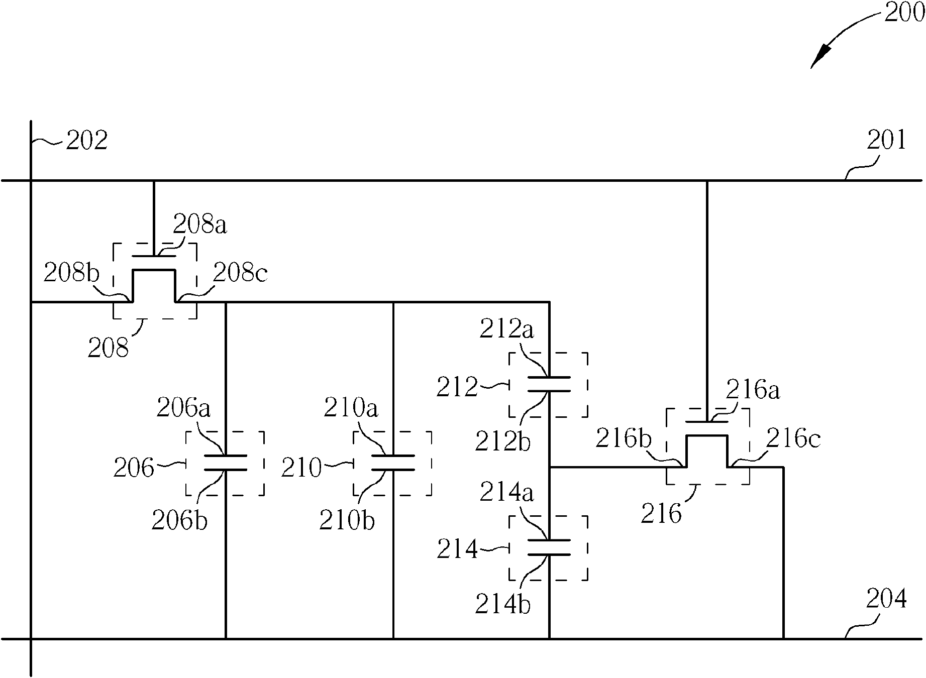
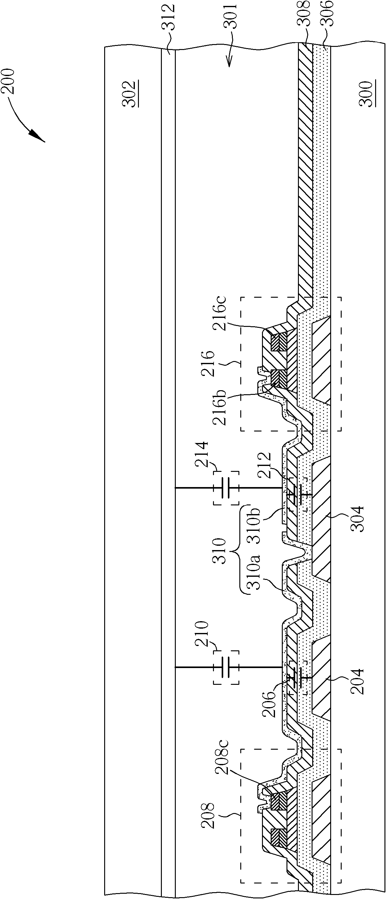
[0021] Please refer to figure 2 and image 3 . figure 2 It is a schematic diagram of an equivalent circuit of the first preferred embodiment of the pixel structure of the present invention, image 3 painted figure 2 The structural cross-sectional schematic diagram of the pixel structure. like figure 2As shown, the pixel structure 200 of the present invention includes a scan line 201, a data line 202, a signal line 204, a storage capacitor 206, a first thin film transistor 208, a first pixel capacitor 210, an adjustment capacitor 212, a first Two pixel capacitors 214 and a second thin film transistor 216 . The storage capacitor 206 includes a first terminal 206a and a second terminal 206b; the first thin film transistor 208 includes a first gate electrode terminal 208a, a first source electrode terminal 208b and a first drain electrode terminal 208c, wherein The first gate electrode terminal 208a is electrically connected to the scan line 201, the first source electro...


PUM


Abstract

The present invention belongs to the field of manufacturing of a liquid crystal display, and particularly provides a pixel structure, which comprises an electrostatic discharging component arranged between an adjusting capacitor and a pixel capacitor. The electrostatic discharging component is used for discharging electrostatic charges accumulated between the adjusting capacitor and the pixel capacitor, so as to reduce the burning of display images.

Description

[0001] This application is a divisional application with an invention title of "pixel structure", the original application number is 200910112488.6, and the filing date is September 10, 2009. 【Technical field】 [0002] The invention relates to a pixel structure, in particular to a pixel structure designed to prevent electrostatic charge accumulation, and belongs to the field of liquid crystal display manufacture. 【Background technique】 [0003] Liquid crystal displays have been widely used in various electronic products, such as mobile phones, personal digital assistants (PDAs) and notebook computers (notebooks). It plays a very important role, and gradually replaces the cathode ray tube (CRT) display to become the mainstream of the market. [0004] Please refer to figure 1 , figure 1 It is a schematic diagram of a traditional capacitive coupling type (Capacitance Coupling Type, C-C type) pixel structure. like figure 1 As shown, the traditional capacitively coupled pixel...

Claims


Application Information

Patent Timeline
IPC IPC(8): G02F1/1362G02F1/1368
Inventor 蔡乙诚康良豪
Owner CPT DISPLAY TECH FUJIAN
Features
  • R&D
  • Intellectual Property
  • Life Sciences
  • Materials
  • Tech Scout
  • Unparalleled Data Quality
  • Higher Quality Content
  • 60% Fewer Hallucinations
Learn More