Check patentability & draft patents in minutes with Patsnap Eureka AI!

Laterally diffused metal oxide semiconductor (LDMOS) and manufacturing method thereof

A technology of epitaxial layer and heavily doped region, which is applied in semiconductor/solid-state device manufacturing, electrical components, transistors, etc., and can solve problems such as leakage of LDMOS devices

Active Publication Date: 2013-03-13
SHANGHAI HUAHONG GRACE SEMICON MFG CORP
View PDF0 Cites 0 Cited by
  • Summary
  • Abstract
  • Description
  • Claims
  • Application Information

AI Technical Summary

Problems solved by technology

Under inductive loads and some special applications, the potential of the drain terminal 181 may be lower than zero potential, while the substrate 10 is always at zero potential. At this time, the PN junction between the drain terminal 181 and the substrate 10 will be forward conducting , which causes leakage current in the LDMOS device

Method used


Image

  • Laterally diffused metal oxide semiconductor (LDMOS) and manufacturing method thereof
  • Laterally diffused metal oxide semiconductor (LDMOS) and manufacturing method thereof

Examples


Embodiment Construction

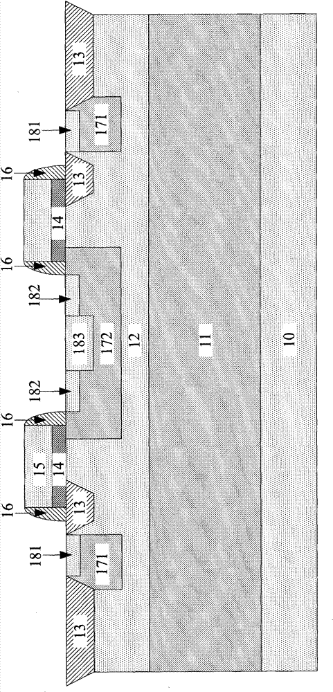
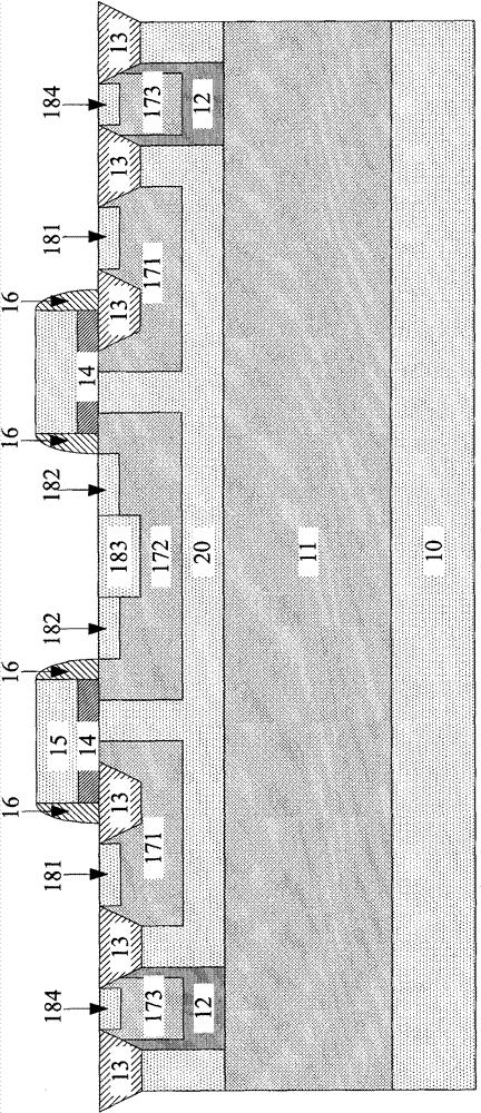
[0027] see figure 2 , the structure of the LDMOS of the present invention is: there is an n-type buried layer 11 on the p-type substrate 10 , and then there is a p-type epitaxial layer 20 above. There are multiple isolation regions 13 in the p-type epitaxial layer 20 , and these isolation regions 13 isolate the n-well 12 , the n-well 171 and the p-well 172 in the p-type epitaxial layer 20 from each other. The bottom of the n-well 12 is in contact with the n-type buried layer 11, that is to say, the depth of the n-well 12 is at least the same as the thickness of the p-type epitaxial layer 20, so the n-well 12 is also called a deep n-well. There is an n well 173 in the n well 12, and the n well 173 will be used as a low-voltage application in the future, so it is also called a low-voltage n well. There is an n-type heavily doped region 184 in the n well 173 . The n-well 171 will also be used as a low-voltage application in the future, so it is also called a low-voltage n-well...


PUM


Abstract

The invention discloses an LDMOS. Two PN junctions isolated are arranged between a drain end (181) and a substrate (10). The P area of the first PN junction is a p-shaped substrate (10), and the N area is an n-shaped buried layer (11). The P area of the second PN junction is a p-shaped epitaxial layer (20), and the N area is an n-pit (171) and an n-shaped heavily doped area (181). The isolating ring consisting of an n-shaped heavily doped area (184), an n pit (173) and an n pit (12) is arranged on the four sides of the LDMOS device. The bottom of the whole isolating ring is contacted with the n-shaped buried layer (11). The invention also discloses a method for manufacturing the LDMOS. The LDMOS and the method can effectively solve the problem that the drain end (181) and the substrate (10) may be connected electrically.

Description

technical field [0001] The invention relates to an LDMOS (laterally diffused MOS, laterally diffused MOS transistor) device. Background technique [0002] see figure 1 , which is a schematic cross-sectional view of an existing LDMOS. There is an n-type buried layer 11 on the p-type substrate 10 , and there is an n-well 12 further above. The depth of the n-well 12 is usually greater than 2 μm, and is also called a deep n-well. There are multiple isolation regions 13 in the n well 12, and these isolation regions 13 isolate the n well 171 and the p well 172 in the n well 12 from each other. There is an n-type heavily doped region 181 in the n well 171, which serves as the drain of the LDMOS device. The p-well 172 has an n-type heavily doped region 182 and a p-type heavily doped region 183, which are connected to serve as the source of the LDMOS device. There is a gate oxide layer 14 on the n-well 12, and a gate 15 on the top, serving as the gate of the LDMOS device. There...

Claims


Application Information

Patent Timeline
Patent Type & Authority Patents(China)
IPC IPC(8): H01L27/088H01L29/78H01L29/06H01L21/8234H01L21/336H01L21/761
CPCH01L29/7823
Inventor 张帅董科
Owner SHANGHAI HUAHONG GRACE SEMICON MFG CORP
Features
  • R&D
  • Intellectual Property
  • Life Sciences
  • Materials
  • Tech Scout
  • Unparalleled Data Quality
  • Higher Quality Content
  • 60% Fewer Hallucinations
Learn More