Touch panel structure and touch display device

A technology of touch display device and touch panel, which is applied in the direction of instruments, electrical digital data processing, and input/output process of data processing, etc., and can solve the problem of large reserved wiring distance, large wiring area, and large occupied space and other problems, to achieve the effect of increasing the sensing sensitivity, reducing the routing area, and increasing the operating area

Inactive Publication Date: 2014-07-16
WINTEK CHINA TECH LTD +1
View PDF5 Cites 1 Cited by
  • Summary
  • Abstract
  • Description
  • Claims
  • Application Information

AI Technical Summary

Problems solved by technology

[0003] Depend on figure 1 It can be seen from the existing diamond-shaped X-axis electrodes 11 and Y-axis electrodes 12 that due to the limitation of geometric shape, the diamond-shaped X-axis electrodes 11 and Y-axis electrodes 12 occupy a relatively large space in the relative range, as shown in the figure As shown, every two X electrode wires 13 need four pitches P, and every two Y electrode wires 14 need four pitches P, forming a large wiring area, and it is impossible to improve the sensitivity of the induction. In addition, the existing electrode and wire layout method , for future applications in high-density writing occasions, for example: when applied to electronic paper writing with smaller electrodes and high precision requirements, there is room for improvement, because the smaller the electrodes, the higher the precision requirements, and the existing layout mode, the reserved routing distance formed by it is relatively large
[0004] At the same time, due to the current design of the electrode layout on the same-plane substrate is mostly rhombus or hexagonal, but limited by the shape of the rhombus and hexagon, the resolution of the sensing electrodes generated is low, and for fingers or touch When the pen is moving, it cannot respond immediately, and for current electronic devices, such as mobile phones, laptops, etc., it is impossible to write text or graphics as densely as paper, forming an obstacle in use

Method used


Image

  • Touch panel structure and touch display device
  • Touch panel structure and touch display device
  • Touch panel structure and touch display device

Examples


Embodiment Construction

[0018] The technical means and effects used by the present invention to achieve the purpose will be described below with reference to the accompanying drawings, and the embodiments listed in the following accompanying drawings are only for auxiliary explanation, so as to facilitate the understanding of the examiners, but the technical means of this case are not limited to the above-mentioned List the attached drawings.

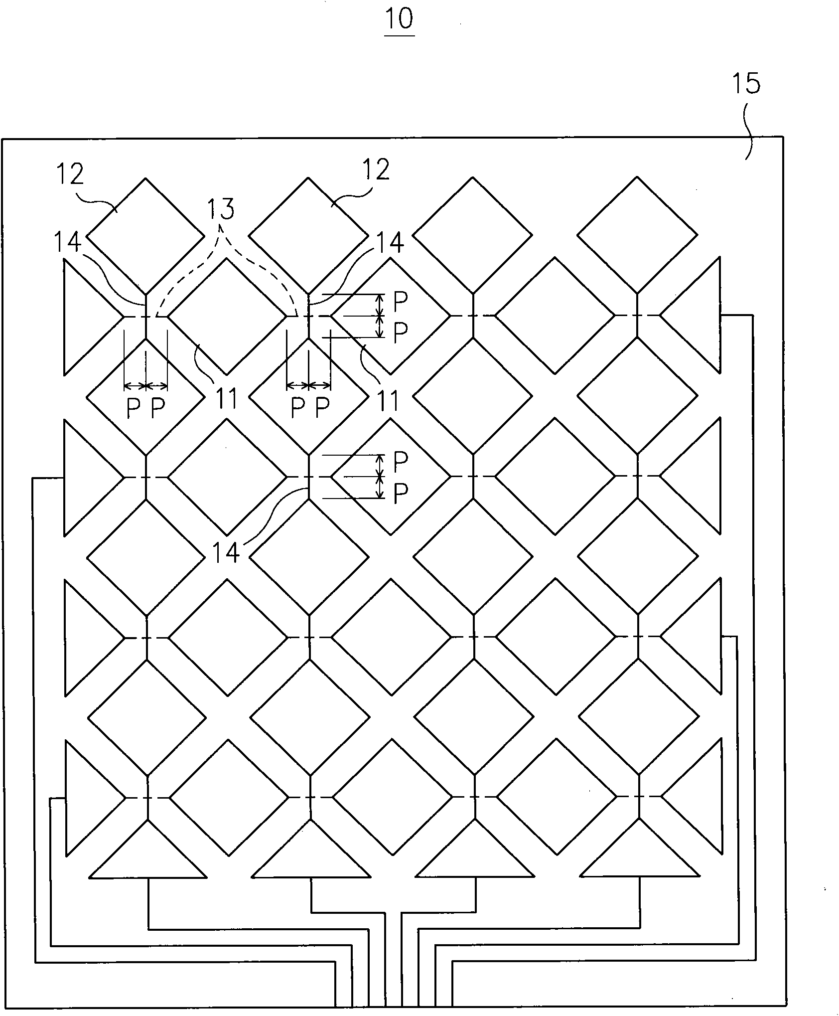
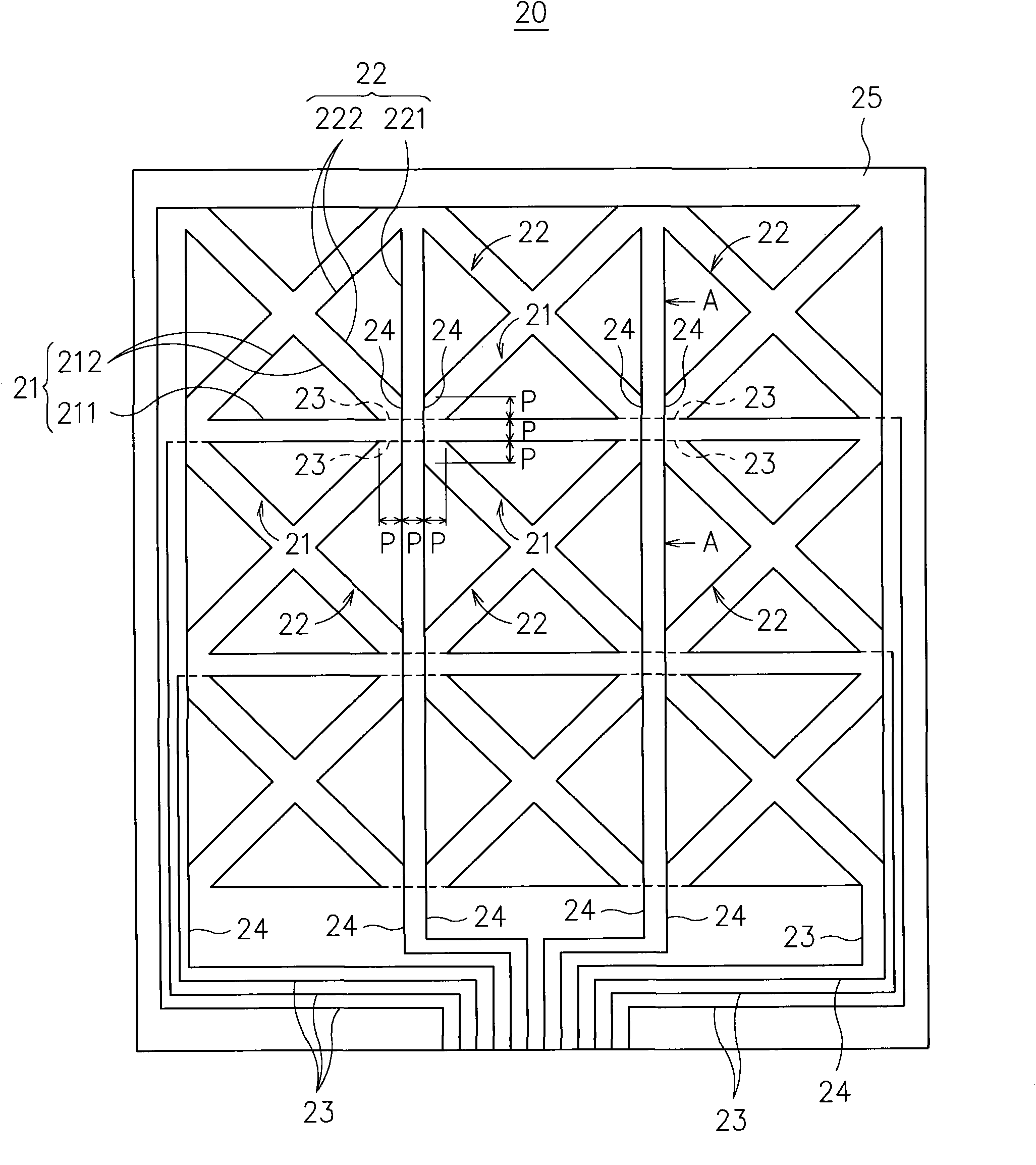
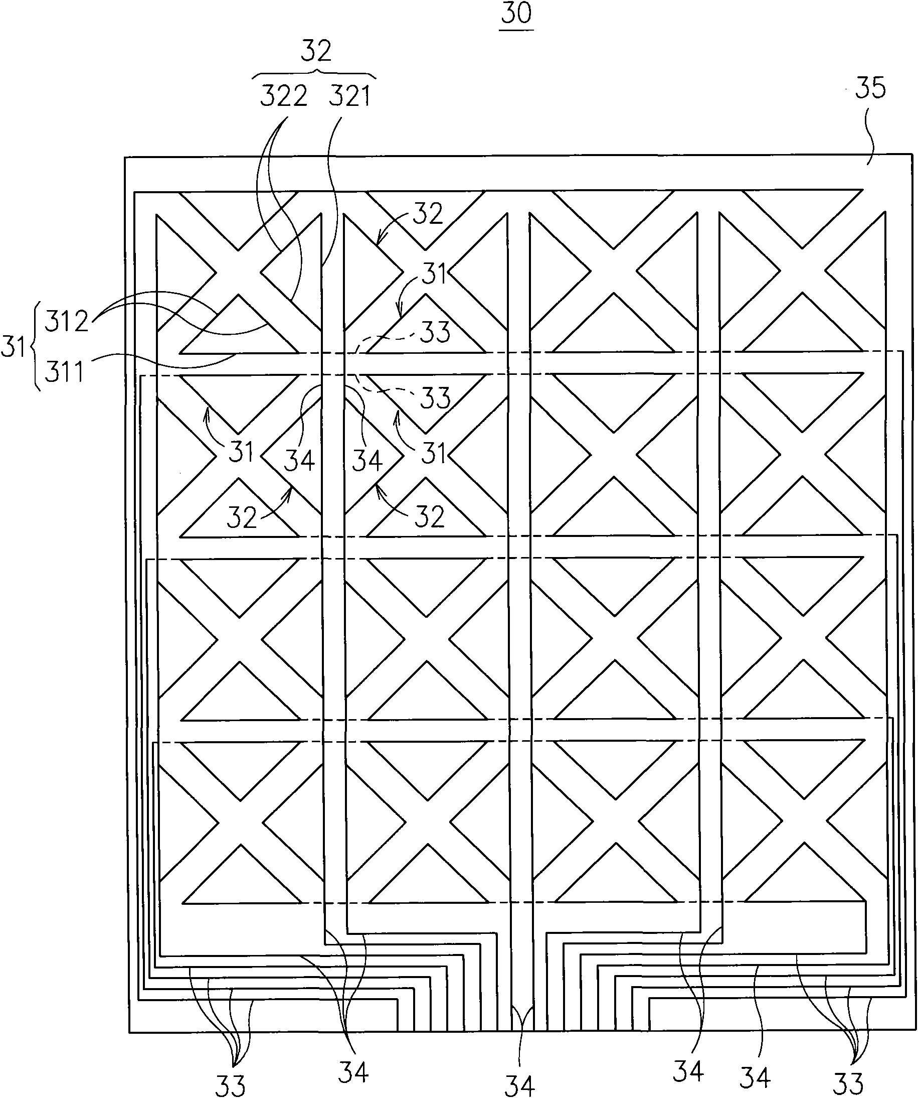
[0019] see figure 2 As shown in the schematic structural diagram of the first embodiment of the present invention, the touch panel 20 includes a substrate 25 on which a plurality of first electrodes 21 and a plurality of second electrodes 22 are arranged. The first electrodes 21 and the second electrodes 22 are are the same shape and size.

[0020] A plurality of first electrodes 21 are arrayed in multiple rows, each row has a plurality of first electrodes 21, and the number of first electrodes 21 in each row is the same, and each first electrode 21 consists...


PUM


Abstract

The invention discloses a touch panel structure and a touch display device. The touch panel structure comprises a substrate, a plurality of lines of first electrodes and a plurality of columns of second electrodes, wherein each first electrode and each second electrode are in a triangular shape; the triangle is provided with a bottom side; each line of first electrodes are connected in series by first leads; two lines of adjacent first electrodes are symmetrical in shape; bottom sides of at least two lines of adjacent first electrodes are relatively and symmetrically arranged; each column of second electrodes are connected in series by second leads; two adjacent columns of second electrodes are symmetrical in shape; the bottom sides of at least two adjacent columns of second electrodes are relatively and symmetrically arranged; the second leads of two columns of second electrodes of which the bottom sides are relatively and symmetrically arranged and the first leads of two lines of first electrodes of which the bottom sides are relatively and symmetrically arranged are mutually staggered; and a display is arranged on one surface of the touch panel structure, which is different from the substrate, so that the touch display device is formed.

Description

technical field [0001] The invention relates to a touch panel structure and a touch display device, in particular to a touch electrode designed as a triangle, which can effectively reduce the routing area, increase the sensing sensitivity, increase the resolution of the touch panel, and reduce the load on the driving integrated circuit. 1. A capacitive touch panel structure and a touch display device capable of enlarging the operating area. Background technique [0002] see figure 1 A structural schematic diagram of an existing capacitive touch panel is shown. In the capacitive touch panel 10, a plurality of X-axis electrodes 11 and a plurality of Y-axis electrodes 12 are alternately arranged on the same surface of a substrate 15, and the plurality of X-axis electrodes 11 are arranged in multiple rows horizontally, and multiple Y-axis electrodes 12 are arranged in multiple columns vertically, and the shapes of X-axis electrodes 11 and Y-axis electrodes 12 are arranged in a ...

Claims


Application Information

Patent Timeline
Patent Type & Authority Patents(China)
IPC IPC(8): G06F3/041
Inventor 邓志容刘锦璋
Owner WINTEK CHINA TECH LTD
Why Eureka
Try Eureka