Manufacturing method of liquid crystal display device and liquid crystal display panel and manufacturing equipment of liquid crystal display device and liquid crystal display panel

A technology for a liquid crystal display panel and a manufacturing method, which is applied in optics, instruments, nonlinear optics, etc., can solve the problems of broken bright spots, affect the display effect, and difficulty of liquid crystal molecules, so as to reduce the broken bright spots, improve the display effect, and reduce dark lines. the effect of

Active Publication Date: 2015-02-18
CHANGSHA HKC OPTOELECTRONICS CO LTD
View PDF4 Cites 0 Cited by
  • Summary
  • Abstract
  • Description
  • Claims
  • Application Information

AI Technical Summary

Problems solved by technology

while in figure 2 In the process of closing the device as shown, the capacitance of the assembled panel is not discharged, and there is still charge in the panel, which makes it difficult for the liquid crystal molecules that have been deflected at a larger angle after being transported by rollers to return to the original state, and then in the After the second UV light irradiation, the larger-angle deflection characteristic of the liquid crystal molecules is preserved, and dark lines are likely to appear on the panel, and broken bright spots are likely to appear when the liquid crystal molecules 12' are poured down, and the display effect is affected.

Method used


Image

  • Manufacturing method of liquid crystal display device and liquid crystal display panel and manufacturing equipment of liquid crystal display device and liquid crystal display panel
  • Manufacturing method of liquid crystal display device and liquid crystal display panel and manufacturing equipment of liquid crystal display device and liquid crystal display panel
  • Manufacturing method of liquid crystal display device and liquid crystal display panel and manufacturing equipment of liquid crystal display device and liquid crystal display panel

Examples


Embodiment Construction

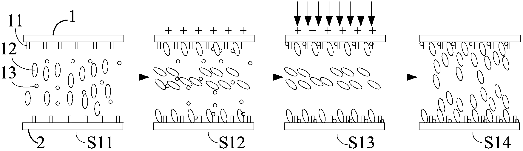
[0027] The manufacturing method of the liquid crystal display panel of the present invention can reduce the appearance of dark lines and broken bright spots of the liquid crystal display panel, and improve the display effect of the liquid crystal display panel.

[0028] The present invention will be described in detail below with reference to the drawings and embodiments.

[0029] refer to Figure 4 , an embodiment of the manufacturing method of the liquid crystal display panel of the present invention comprises steps:

[0030] Step S101: Applying a voltage between the upper and lower substrates of the liquid crystal display panel to form an electric field.

[0031] For the first UV light irradiation process in the PSVA liquid crystal display panel production process, by means of the electrode structure in the upper and lower substrates on both sides of the liquid crystal molecular layer, the electrode structure is turned on and a voltage is applied to it, so that the upper a...


PUM


Abstract

A producing method of a liquid crystal display panel comprises: adding voltage between an upper substrate and a lower substrate of the liquid crystal display panel so as to form an electric field; enabling liquid crystal molecules between the upper substrate and the lower substrate to form a pretilt angle under the electric field; and releasing the voltage between the upper substrate and the lower substrate where the pretilt angle of the liquid crystal molecules is formed. Further provided are a producing method of a liquid crystal display device and a producing device of a liquid crystal display panel. In the foregoing manner, occurrence of dark fringe of the liquid crystal display panel can be reduced, probability that fragmentary light spots exist on the liquid crystal display panel can be reduced, and displaying effects can be improved.

Description

technical field [0001] The invention relates to the technical field of liquid crystal display, in particular to a liquid crystal display device, a manufacturing method and manufacturing equipment of a liquid crystal display panel. Background technique [0002] With the continuous development of liquid crystal display technology, the wide viewing angle technology in liquid crystal display technology has also risen to a new level. As the most direct basis for judging the performance of a display panel, wide viewing angle technology is not only related to the viewing angle of the display panel, but also directly affects other parameters such as the response time and brightness of the display panel. In order to obtain better display effects, the requirements for wide viewing angle technology are getting higher and higher. [0003] Wide viewing angle technologies mainly include TN+Film (Twisted Nematic+Film, twisted nematic liquid crystal + viewing angle expansion film), VA (Ver...

Claims


Application Information

Patent Timeline
Patent Type & Authority Patents(China)
IPC IPC(8): G02F1/1337G02F1/1333
CPCG02F1/133711G02F1/1393G02F2001/133746G02F2001/13373G02F2001/13775G02F2202/023G02F1/13373G02F1/133746G02F1/13775
Inventor 王金杰陈政鸿
Owner CHANGSHA HKC OPTOELECTRONICS CO LTD
Why Eureka
Try Eureka