Hard microstrip circuit electroplating fixture

A microstrip circuit and electroplating fixture technology, applied in the electrolysis process, electrolysis components, etc., can solve the problems of easily damaged substrates, poor electrical contact at points, inconsistent tightening screws, etc.

Active Publication Date: 2012-11-14
CHINA ELECTRONIS TECH INSTR CO LTD
View PDF8 Cites 10 Cited by
  • Summary
  • Abstract
  • Description
  • Claims
  • Application Information

AI Technical Summary

Problems solved by technology

[0005] (1) The thickness of the hard microstrip circuit substrate ranges from 0.1 to 1 mm. When the substrate is very thin, it is easy to damage the substrate when fastening screws or binding copper wires;
[0006] (2) Due to the inconsistent force when tightening the screws, some points have good electrical contact, and some points have poor electrical contact;
[0007] (3) It is troublesome to load and unload the plated parts, and the efficiency is low;
[0008] (4) If the ground metal is required on the back, it generally does not need to have the same thickness as the front transmission line, but when using traditional electroplating fixtures, the back ground metal is usually plated with the same thickness as the front transmission line, resulting in waste of precious metals

Method used


Image

  • Hard microstrip circuit electroplating fixture
  • Hard microstrip circuit electroplating fixture
  • Hard microstrip circuit electroplating fixture

Examples


Embodiment Construction

[0017] The preferred embodiments of the present invention will be described in detail below in conjunction with the accompanying drawings; it should be understood that the preferred embodiments are only for illustrating the present invention, rather than limiting the protection scope of the present invention.

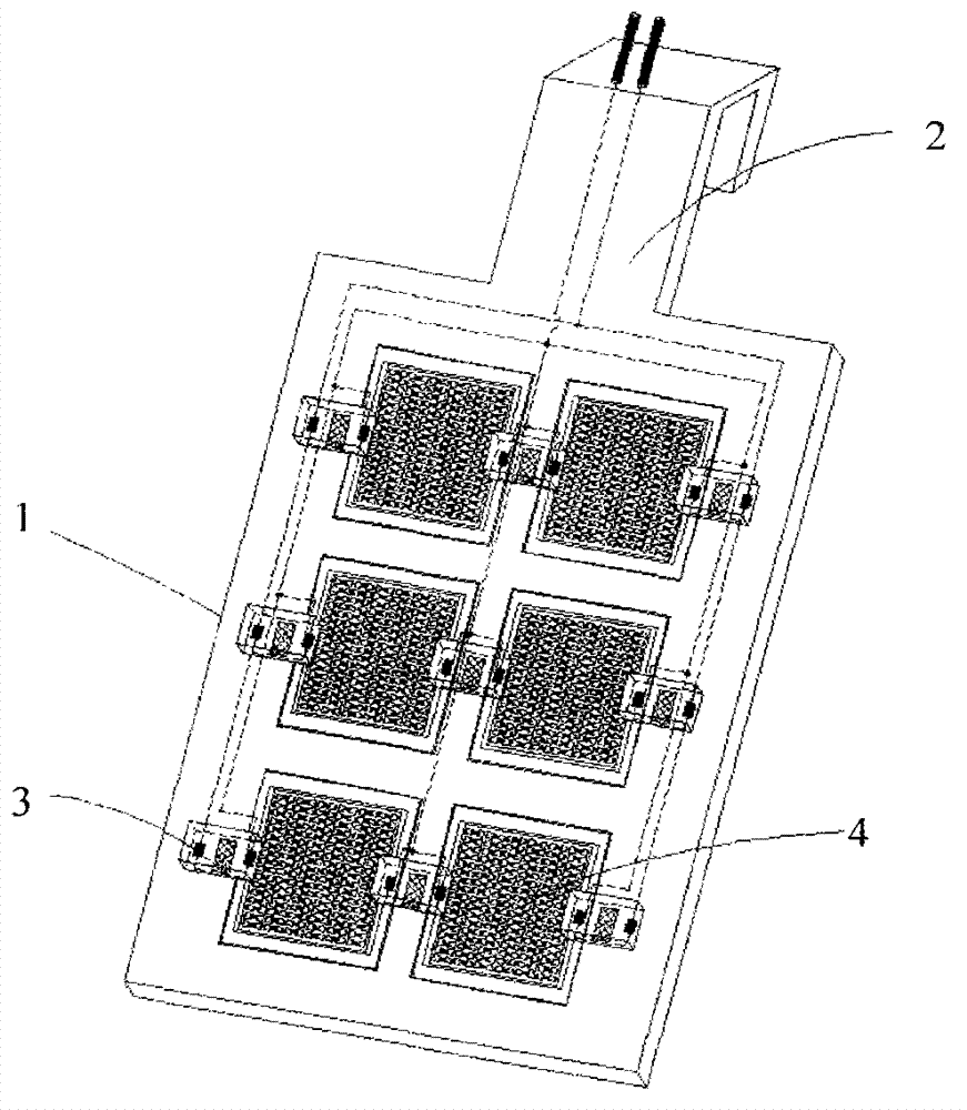
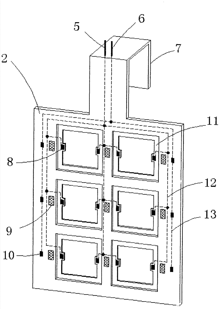
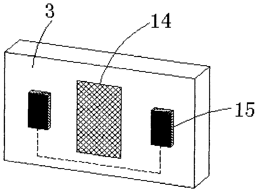
[0018] A rigid microstrip circuit electroplating fixture, including a main body and conductive electromagnetic force fingers, the main body includes a plurality of orderly arranged substrate frames, electrode I, electrode II and magnet I, and the conductive electromagnetic force finger includes electrode III and magnet II, the magnet I on the main body and the magnet II on the conductive electromagnetic force clamp finger attract each other so that the conductive magnetic force clamp finger fixes the hard microstrip circuit substrate in the substrate frame, the electrode I on the main body and the hard microstrip circuit The reverse side or the front side of the strip ci...


PUM

PropertyMeasurementUnit
thicknessaaaaaaaaaa

Abstract

The invention relates to a hard microstrip circuit electroplating fixture, which comprises a main body and conductive magnetic clamping fingers. The main body comprises hard microstrip circuit substrate frames, electrodes I, electrodes II and magnets I. Each conductive magnetic clamping finger comprises electrodes III and a magnet II. The magnets I on the main body and the magnets II on the conductive magnetic clamping fingers attract each other to enable the conductive magnetic clamping fingers to fix hard microstrip circuit substrates in the hard microstrip circuit substrate frames on the main body. The electrodes I on the main body are electrically connected with back surfaces or front surfaces of hard microstrip circuits. The electrodes II on the main body are electrically connected with the front surfaces or the back surfaces of the hard microstrip circuits through the electrodes III on the conductive magnetic clamping fingers. All electrodes I on the main body are electrically connected with a lead-out electrode I. All electrodes II on the main body are electrically connected with a lead-out electrode II. Compared with the existing electroplating fixture, the hard microstrip circuit electroplating fixture provided by the invention has the advantages that very thin electroplated parts can be prevented from being damaged; the consistency of electric contact is good; the loading and unloading efficiency of the electroplated parts is high; and the precious metal is saved.

Description

technical field [0001] The invention relates to an electroplating fixture, in particular to a rigid microstrip circuit electroplating fixture. Background technique [0002] In the field of microwave hybrid integrated circuits, common types of microwave transmission lines include coaxial lines, microstrip lines, striplines, and waveguides. Microstrip lines are the most used in microwave circuits, and the materials that make up microstrip lines are metals and dielectrics. According to different dielectric materials, microstrip lines can be divided into hard (material) microstrip lines and soft (material) microstrip lines. In the microwave field, the current tends to flow near the outer surface of the wire, and this phenomenon intensifies as the frequency increases, which is commonly referred to as the "skin effect". In order to reduce the influence of skin effect, the conductor thickness should be at least 3 times the skin depth. In order to simplify the process, save preci...

Claims


Application Information

Patent Timeline
Patent Type & Authority Applications(China)
IPC IPC(8): C25D17/06
Inventor 宋振国路波王斌
Owner CHINA ELECTRONIS TECH INSTR CO LTD
Why Eureka
Try Eureka