Pixel circuits for active matrix oled displays

A technology of circuit devices and driving circuits, applied to static indicators, instruments, electrical components, etc., to achieve high-resolution effects

Active Publication Date: 2016-01-20
FRAUNHOFER GESELLSCHAFT ZUR FOERDERUNG DER ANGEWANDTEN FORSCHUNG EV
View PDF7 Cites 0 Cited by
  • Summary
  • Abstract
  • Description
  • Claims
  • Application Information

AI Technical Summary

Problems solved by technology

[0017] The field of application of currently available OLED microdisplays is limited to unidirectional image reproduction microdisplays

Method used


Image

  • Pixel circuits for active matrix oled displays
  • Pixel circuits for active matrix oled displays
  • Pixel circuits for active matrix oled displays

Examples


Embodiment Construction

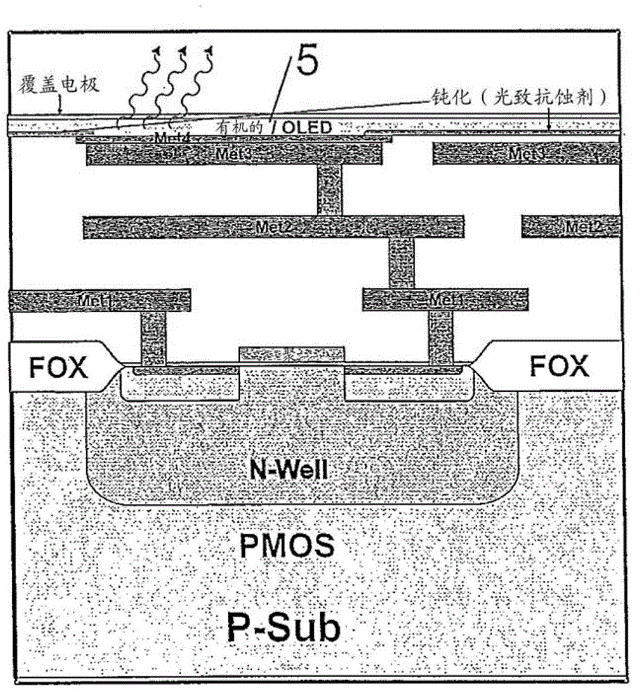
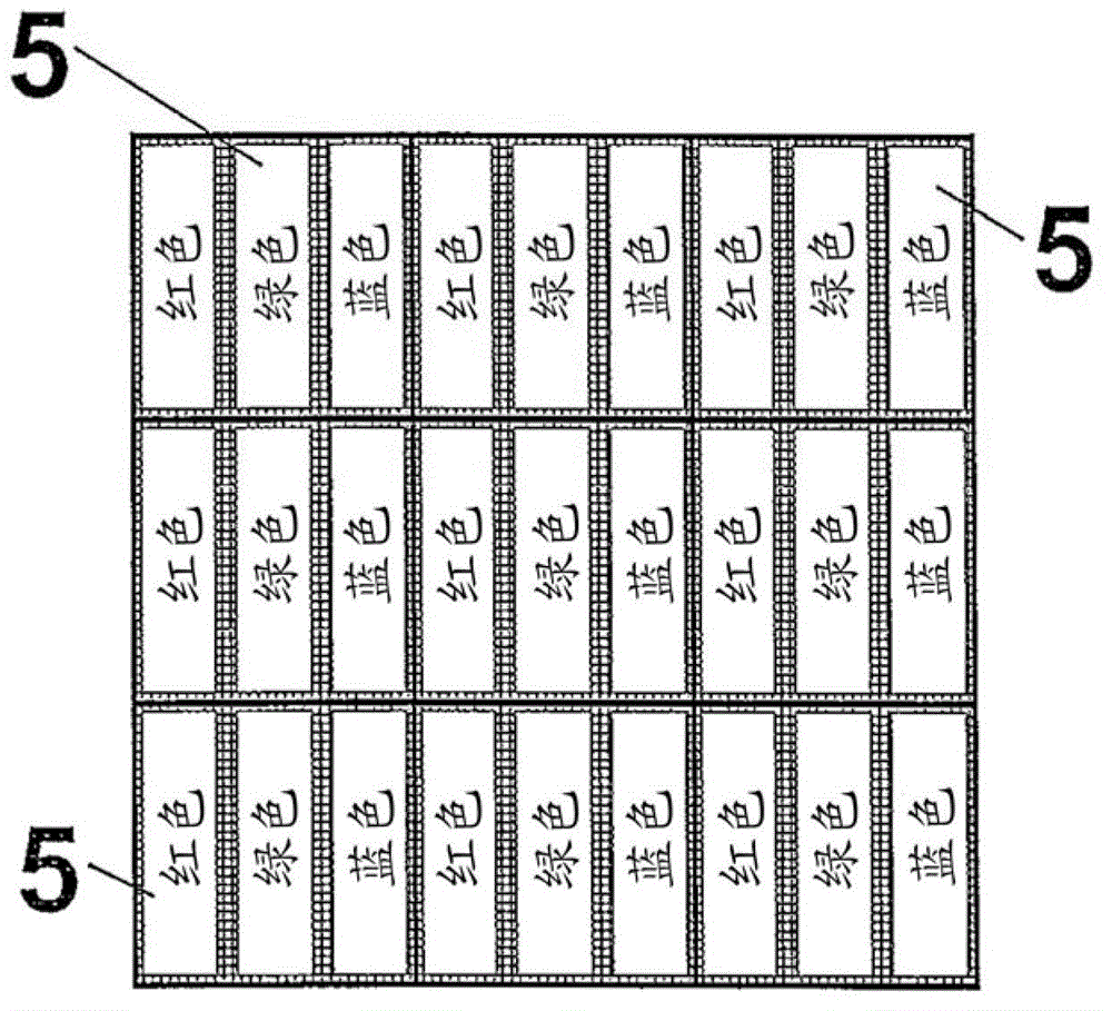
[0046] The microdisplay with organic light emitting diodes 5 is preferably designed such that it comprises an organic layer (OLED) that emits light according to the current flow on the top metal plane on the CMOS substrate. They can be activated locally, ie as so-called pixels, in which a current flows locally through the organic light-emitting diode 5 via the electrodes of the organic light-emitting diode 5 . The active and passive components responsible for controlling each organic light emitting diode 5 (as regular transistors and capacitors) can be located below the electrodes in a matrix-like arrangement of pixel cells. figure 1 A schematic cross-sectional view of an OLED microdisplay is shown.

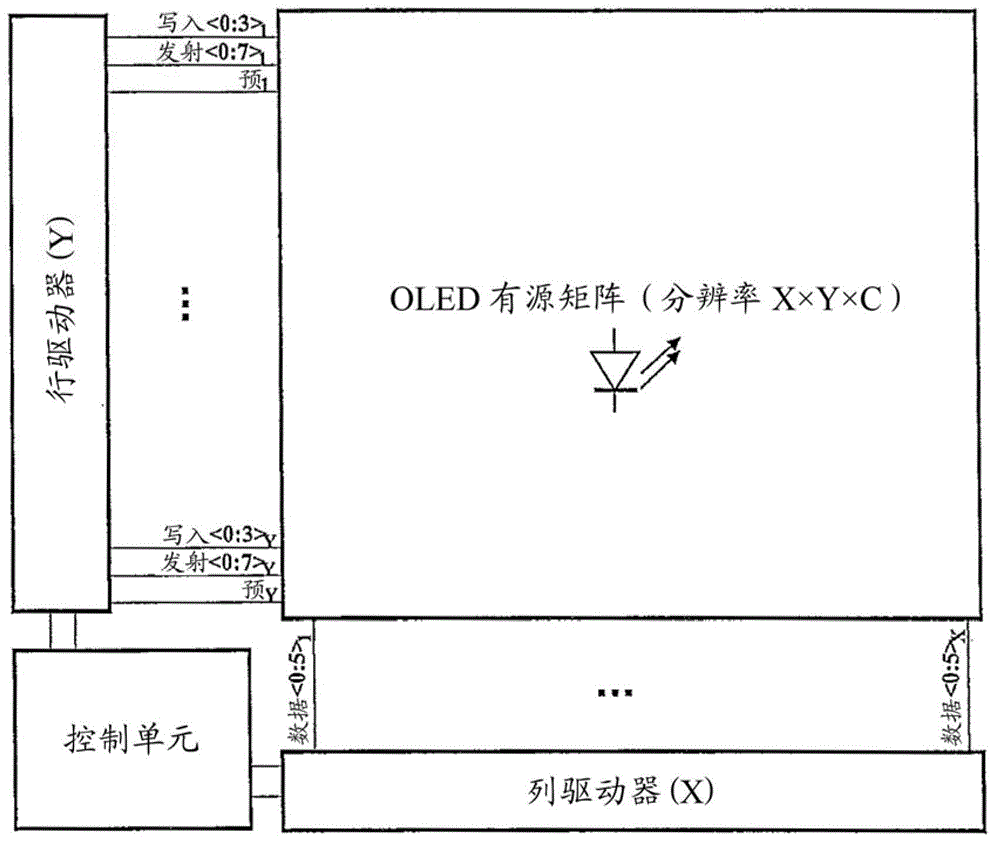
[0047] Such as figure 2 As shown, the individual accumulators for the organic light-emitting diodes 5 arranged in rows and columns are written to by corresponding circuits. In this regard, the image input data is received by the electronic control mechanism. The electronic co...


PUM


Abstract

A circuit arrangement for organic light-emitting diodes can be arranged in a two-dimensional matrix. It can in particular be used with microdisplays. It can allow a wide influencing of the brightness of the electromagnetic radiation emitted by the organic light-emitting diodes. Every organic light-emitting diode can be controlled by means of a storage circuit, a sense amplifier and a driver circuit using the circuit arrangement. The driver circuit can be formed by at least three transistors connected in series and a further output transistor whose drain is connected to the anode of the respective organic light-emitting diode. In this respect, the transistor acting as the driver can have a constant electric operating voltage LVDD applied at its source and a further likewise constant electric operating voltage Vdrive is applied to its gate. The drain of the first transistor to the source of the following transistor connected to it in series and the two gates of the following transistors which form a switch and are connected in series are connected to the output of the sense amplifier and are acted on by its electric output voltage VSenseOut. The drains of the two transistors forming the switch are connected to the source of the output transistor whose gate is connected to ground potential or to which negative electric voltage is applied.

Description

technical field [0001] The invention relates to a circuit arrangement for organic light-emitting diodes arranged in a two-dimensional matrix. Background technique [0002] The ever-increasing number of information systems and environmental impacts provides information that people request as well as information that they do not. In this regard, the mobile display of information has become increasingly important. In this regard, microdisplays (i.e., very small displays with an image diagonal smaller than or equal to 20mm) provide the ability to display high-resolution images in a user-specific manner (i.e., for only one user or for multiple users) Possibility to display photographic information and video information. The field of application of microdisplays can be seen as near-eye applications. They include, for example, video glasses that can be connected to mobile multimedia devices (smartphones or mobile audio and video players). These video glasses can be used for mob...

Claims


Application Information

Patent Timeline
Patent Type & Authority Patents(China)
IPC IPC(8): G09G3/3233
CPCG09G3/2018G09G3/3233G09G3/3258G09G3/3291G09G2300/0809G09G2300/0814G09G2300/0852G09G2300/0861G09G2310/0251G09G2310/0262G09G2320/0626G09G2320/0633G09G2320/064G09G2330/04H05B47/10G09G3/32
Inventor 丹尼尔·克雷耶托马斯·普雷斯博格尔
Owner FRAUNHOFER GESELLSCHAFT ZUR FOERDERUNG DER ANGEWANDTEN FORSCHUNG EV
Why Eureka
Try Eureka