Universal nonvolatile memory control device for system on chip

A non-volatile storage and non-volatile technology, applied in the field of system chip integrated design, can solve the problems of complex design process and poor compatibility of non-volatile memory, and achieve the effect of simplifying the design process and good compatibility

Active Publication Date: 2013-03-27
C SKY MICROSYST CO LTD
View PDF3 Cites 12 Cited by
  • Summary
  • Abstract
  • Description
  • Claims
  • Application Information

AI Technical Summary

Problems solved by technology

[0005] In order to overcome the shortcomings of poor compatibility and complicated design process of the existing non-volatile memory, the present

Method used


Image

  • Universal nonvolatile memory control device for system on chip
  • Universal nonvolatile memory control device for system on chip
  • Universal nonvolatile memory control device for system on chip

Examples


Embodiment Construction

[0038] The present invention will be further described below in conjunction with the accompanying drawings.

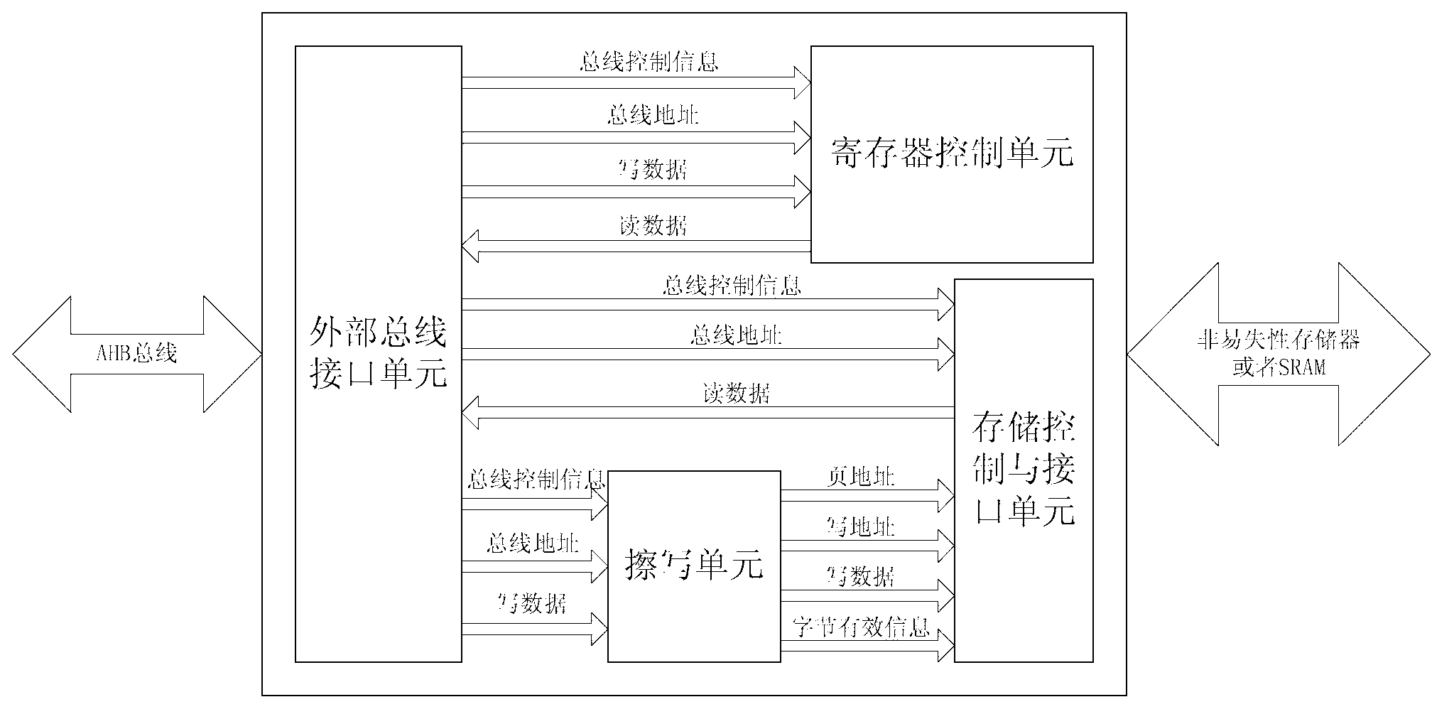
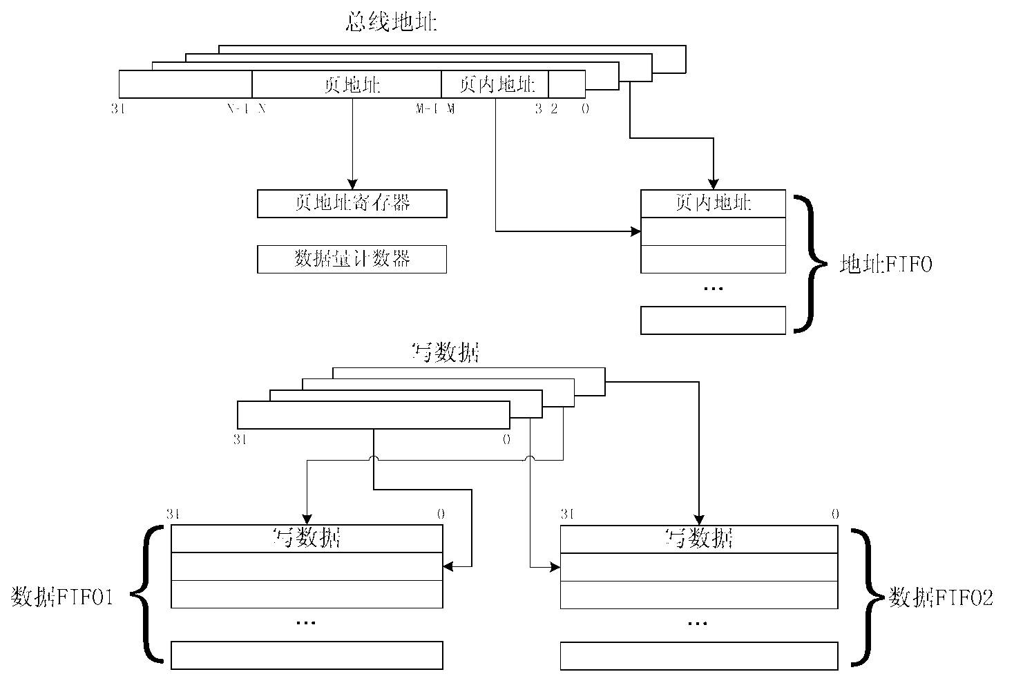
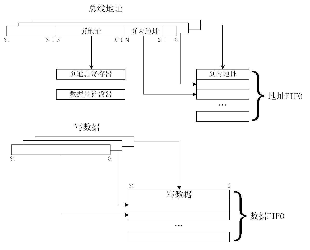
[0039] refer to Figure 1~Figure 12 A general non-volatile memory control device for system chip integration, comprising an external bus interface unit, a register control unit, an erasing unit, and a storage control and interface unit. Through the cooperative work of these units, compatibility with various non-volatile memories and simulation of various non-volatile memories are realized:

[0040]The external bus interface unit is responsible for collecting the control signals and data of the external bus and analyzing them: if it is an access control register, the bus signal is transmitted to the register control unit; if the non-volatile memory unit is read, the bus signal is transmitted to For the storage control and interface unit, the read operation of the non-volatile storage unit is realized; if the non-volatile storage unit is written, the bus signal is trans...


PUM


Abstract

The invention relates to a universal nonvolatile memory control device for a system on a chip. The control device comprises an external bus interface unit, a register control unit, an erasing unit and a storage control and interface unit. The external bus interface unit is used for collecting control signals and data of an external bus as well as analyzing the signals and data; the register control unit is used for read-write control of all registers, wherein the register data is transmitted to the storage control and interface unit for use by a finite-state machine of the storage control and interface unit; the erasing unit is used for processing bus signals transmitted by the external bus interface unit; the storage control and interface unit comprises two finite-state machines: one is a write data width conversion state machine, while the other is a master control state machine for read, write and erase control of various nonvolatile memories. The invention provides the universal nonvolatile memory control device for the system on the chip good in compatibility and simplified in design process.

Description

technical field [0001] The invention relates to the field of system chip (SoC) integration design, in particular to a highly compatible universal non-volatile memory control device for system chip integration. Background technique [0002] With the continuous improvement of the manufacturing level of integrated circuits, designers can integrate complex systems with millions of gates on a single chip, that is, System-On-Chip. In recent years, SoC has become the mainstream direction of today's integrated circuit design. In order to meet the needs of more and more diverse practical applications, as an important device for storing data, various types of non-volatile memory (Non-Volatile- Memory) is also being gradually integrated into the SoC chip. These non-volatile memories include OTP, EEPROM, FLASH, etc. [0003] Different types of non-volatile memories usually have different control signals and timing requirements. Therefore, for different non-volatile memories, it is oft...

Claims


Application Information

Patent Timeline
IPC IPC(8): G06F13/16
Inventor 葛海通王钰博马德严晓浪
Owner C SKY MICROSYST CO LTD
Why Eureka
Try Eureka