Supercharge Your Innovation With Domain-Expert AI Agents!

Magnetron sputtering device

A magnetron sputtering device and magnet technology, applied in sputtering plating, ion implantation plating, coating, etc., can solve the problems of complexity, heavy weight, and 10 large magnet units, and achieve the effect of reducing manufacturing costs

Active Publication Date: 2013-05-15
CANON ANELVA CORP
View PDF5 Cites 3 Cited by
  • Summary
  • Abstract
  • Description
  • Claims
  • Application Information

AI Technical Summary

Problems solved by technology

In recent large-scale sputtering devices such as substrates with a size exceeding 1 m, the magnet unit 10 is also large and heavy, so that the mechanism for moving the magnet unit 10 to the target side becomes large and complicated, and there are difficulties in device manufacturing. The problem of high cost

Method used


Image

  • Magnetron sputtering device
  • Magnetron sputtering device
  • Magnetron sputtering device

Examples


no. 1 Embodiment approach )

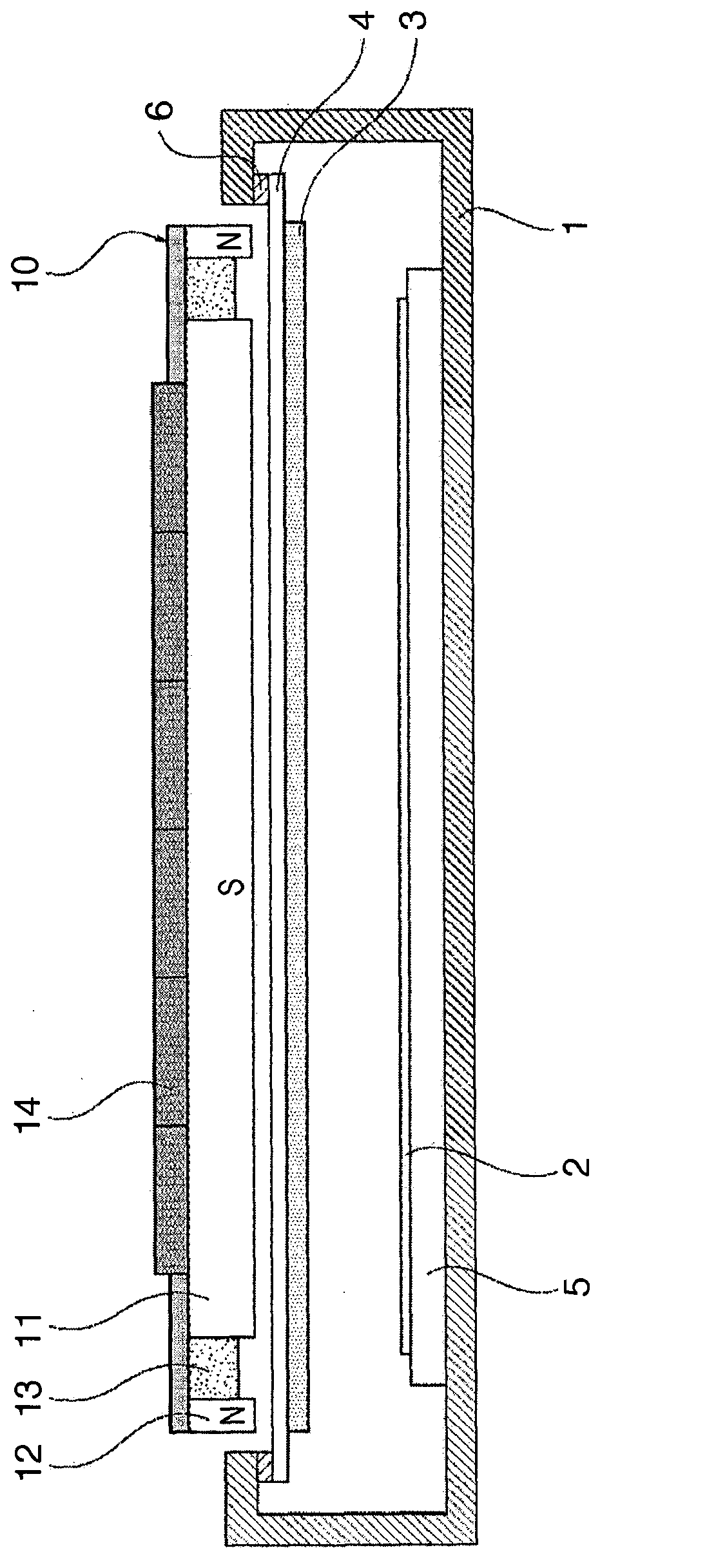
[0043] Next, a magnetron sputtering apparatus according to a first embodiment of the present invention will be described with reference to the drawings. figure 1 The schematic structure of the magnetron sputtering apparatus concerning this embodiment is shown in . A substrate 2 is placed on a substrate rack 5 in the chamber 1 . The chamber 1 is evacuated to a vacuum by an exhaust pump not shown, and a process gas such as Ar gas is supplied through a gas pipe not shown to form a predetermined pressure.

[0044] The target 3 is disposed above and facing the substrate 2 . The cathode 4 enables the target 3 to be mounted on the mounting surface, and the cathode 4 is installed in the cavity 1 through the insulator 6 .

[0045] In this embodiment, an example is shown in which the rear surface side of the cathode 4 where the target 3 can be mounted is exposed to the air. The cathode 4 is connected to an unillustrated DC power supply. On the back side of the cathode 4, a magnet u...

no. 2 Embodiment approach )

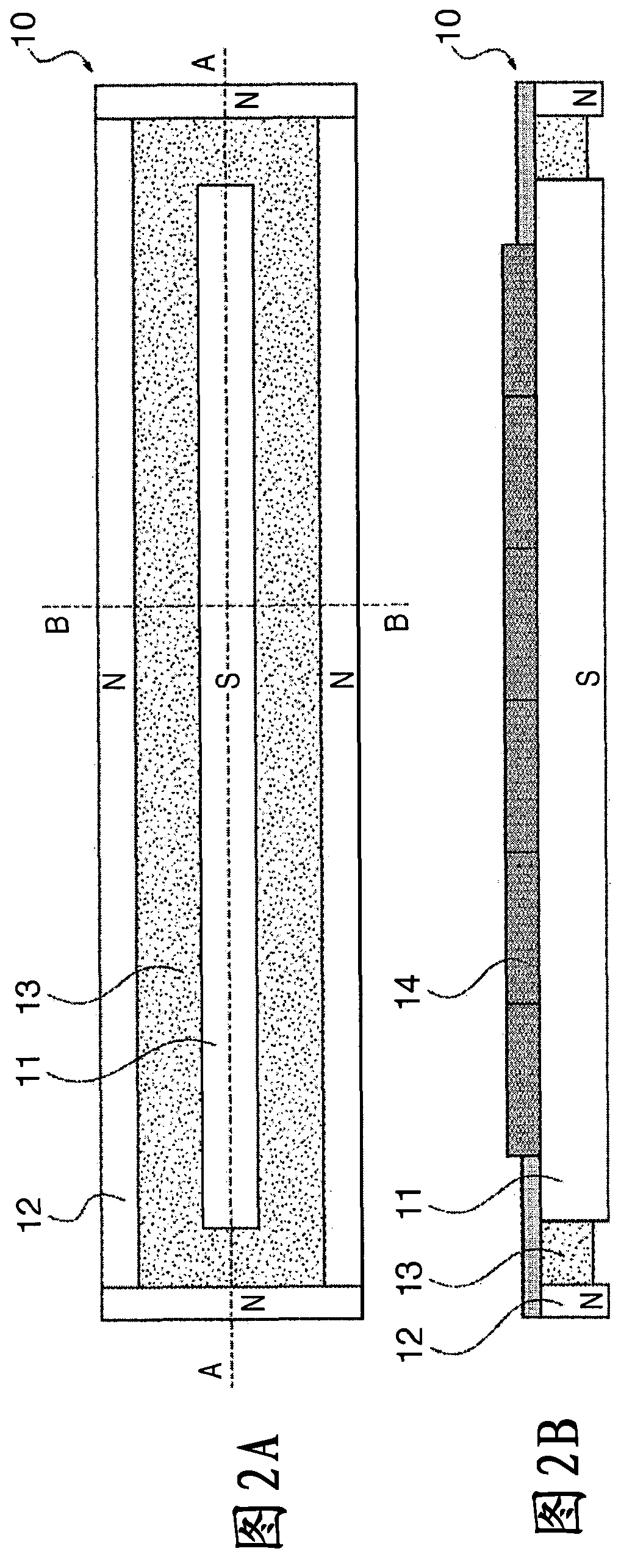
[0066] Next, a second embodiment of the present invention will be described. exist Figure 7A The inner magnet 11 and the outer magnet 12 of the magnet unit 10 shown have magnets 15 made of ferromagnets such as iron and SUS430 respectively connected to the magnetic poles on the opposite side to the target 3 by adhesive or the like. A magnet 15 connected to the inner magnet 11 and the outer magnet 12 is connected into the magnetic circuit via the yoke 14 .

[0067] The yoke 14 is not fixed by an adhesive or the like, but is attached only by the attraction force (magnetic force) of the magnets (inner magnet 11 , outer magnet 12 ), and thus can be removed. There is a non-magnetic body 13 between the inner magnet 11 and the outer magnet 12, and the magnet 15 and the non-magnetic body 13 are fixed by an adhesive, bolts, or the like.

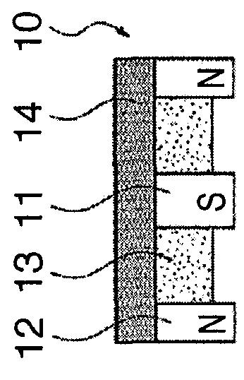
[0068] The structure of the magnet unit 10 without the yoke 14 is in Figure 7B shown in . Since the magnet 15 and the non-magnet 13 are fixed, t...


PUM


Abstract

The invention provides a magnetron sputtering device. The magnetron sputtering device is configured to have a magnet unit which is capable of moving along the back side of the negative pole of an installed target. The magnetron sputtering device is characterized in that the magnet unit is provided with an inner magnet which is formed by a permanent magnet and enables the pole face of a pole to face toward the negative pole; an outer magnet which encloses the inner magnet and enables the pole face of the pole opposite to the inner magnet to face toward the negative pole; and a plate-shaped yoke which is made of strong magnetic materials and is arranged at one sides, opposite to the negative pole, of the inner magnet and the outer magnet, as well as connecting the poles of the inner magnet and the outer magnet. The yoke has a thin part compared with the thickness of other parts. The thin part is configured to be the part between the outer magnet and the inner magnet in the length direction of the moving direction of the magnet unit.

Description

[0001] This application is a divisional application of the invention patent application with the application number 201110072752.5, the application date is March 25, 2011, and the invention title is "magnetron sputtering device and sputtering method". technical field [0002] The invention relates to a magnetron sputtering device. Background technique [0003] As a method of forming a thin film on a substrate for a solar cell, a semiconductor wafer, or the like, there is a sputtering method. In particular, a magnetron sputtering apparatus in which a magnet is disposed on the back side of a cathode on which a target is mounted is excellent in stability of film formation and easy to increase the size of the target, and thus is widely used. In order to improve productivity, attempts have been made to increase the number of substrates that can be produced from one target by making the etching depth of the target as uniform as possible. In addition, in order to improve the unifo...

Claims


Application Information

Patent Timeline
Patent Type & Authority Applications(China)
IPC IPC(8): C23C14/35
CPCC23C14/3407C23C14/35C23C14/52H01J37/3408H01J37/3414H01J37/3455
Inventor 佐佐木雅夫
Owner CANON ANELVA CORP
Features
  • R&D
  • Intellectual Property
  • Life Sciences
  • Materials
  • Tech Scout
  • Unparalleled Data Quality
  • Higher Quality Content
  • 60% Fewer Hallucinations
Learn More