Electron beam exposure patterning method on an insulating substrate
What is AI technical title?
AI technical title is built by PatSnap AI team. It summarizes the technical point description of the patent document.
A technology of electron beam exposure and insulating substrate, applied in the field of microelectronics, can solve the problems of electron beam deflection, exposure pattern shift, distortion deformation, etc., and achieve the effect of solving the charge accumulation and facilitating the peeling process
Inactive Publication Date: 2016-08-17
SHANGHAI INST OF MICROSYSTEM & INFORMATION TECH CHINESE ACAD OF SCI
View PDF3 Cites 0 Cited by
Summary
Abstract
Description
Claims
Application Information
AI Technical Summary
This helps you quickly interpret patents by identifying the three key elements:
Problems solved by technology
Method used
Benefits of technology
Problems solved by technology
Generally, electron beam exposure is suitable for semiconductor or conductor materials, and when an insulating material is used as the substrate, when the thickness of the insulating layer on the surface of the sample exceeds 20 microns, when the electron beam spot hits the sample, the charges gather on the surface of the sample to generate an electric field and cause electrons to The beam is deflected, causing the exposure pattern to shift or distort
This poses a severe challenge to the fabrication of micro-nano devices on insulating substrates
Method used
Image
Click on the blue label to locate the original text in one second.
Reading with bidirectional positioning of images and text.
Examples
Embodiment 1
[0052] The invention provides an electron beam exposure patterning method on an insulating substrate, which specifically includes the following steps:
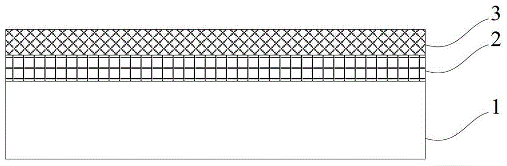
[0053] see figure 1 As shown, an insulating substrate 1 is provided, and the upper surface of the insulating substrate 1 is spin-coated with PMMA1 type electron beam photoresist 2 by using an automatic glue leveler. About 10s, then fast 4000rpm, the time is about 45s, and then it can be dried at a temperature of about 180°C. Then spin-coat PMMA2 type electron beam photoresist 3, the rotation speed is set to slow at 500rpm for about 10s, then fast at 4000rpm for about 45s, and then dried at a temperature of about 180°C. The obtained structure diagram is as follows figure 1 shown.
[0054] Wherein, the thickness of the insulating substrate can be more than 10 microns, and the material of the insulating substrate can be SiO 2 、Al 2 o 3 Or MgO, etc., in this embodiment, choose SiO 2 substrate. In this step, a cleaning st...
Embodiment 2
[0062] This embodiment provides another electron beam exposure patterning method on an insulating substrate, which specifically includes the following steps:
[0063] First, see Figure 6 As shown, an insulating substrate 10 is provided, and the PMMA1 type electron beam photoresist 20 is spin-coated by an automatic coating machine. Left and right drying, the obtained structure graph is as follows Figure 6 shown.
[0064] The thickness of the insulating substrate 10 can exceed 10 microns, and the substrate can be SiO 2 , Al2O 3 , MgO, etc., in this embodiment, preferably SiO 2 substrate. Before this step, a cleaning step of the insulating substrate 10 is also included. In this embodiment, a standard RCA process is used to clean the SiO 2 substrate.
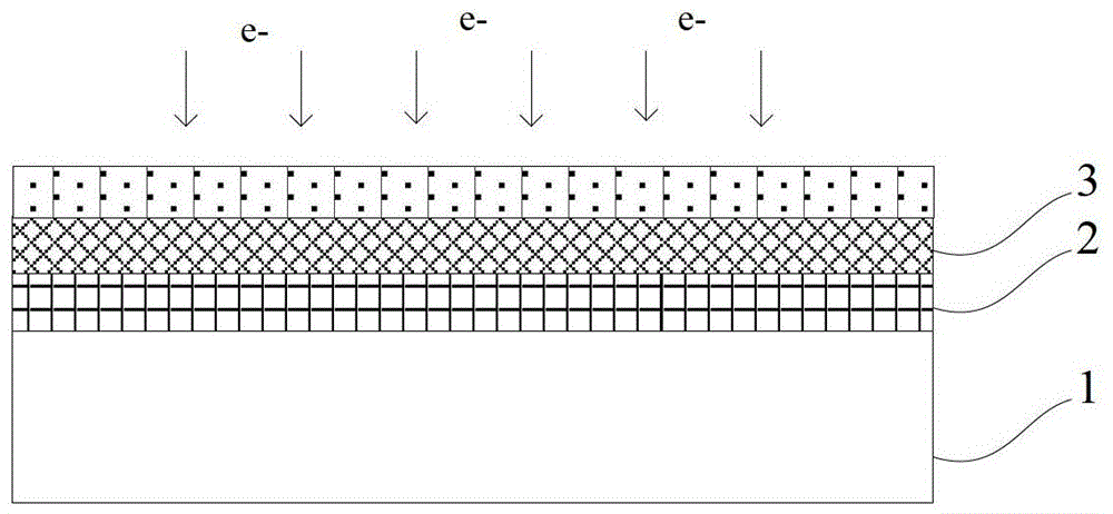
[0065] Next, deposit metal thin film 40 on the insulating substrate 10 of spin-coating PMMA1 type electron beam photoresist 20, then adopt automatic glue leveling machine to spin coat PMMA2 type electron beam photoresist 30...
PUM
Property
Measurement
Unit
thickness
aaaaa
aaaaa
thickness
aaaaa
aaaaa
thickness
aaaaa
aaaaa
Abstract
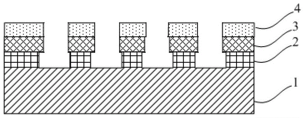
The invention provides an electron beam exposure patterning method on an insulating substrate. The electron beam exposure patterning method comprises the following steps of: 1) providing the insulating substrate; 2) coating electron beam photoresist on the insulating substrate in a rotating way; 3) forming a metal film on the upper surface of the electron beam photoresist; 4) carrying out electron beam exposure to obtain a required photoetching pattern; 5) depositing to form a metal layer on the obtained photoetching pattern, so as to form a metal electrode; and 6) stripping, and removing the photoresist and redundant metal, so as to obtain a required metal pattern. According to the electron beam exposure patterning method on the insulating substrate, the double-layer electron beam photoresist is adopted for the exposure, an undercut structure beneficial to a follow-up metal stripping technology can be obtained by developing, discontinuous metal films are formed on the double-layer electron beam photoresist in an evaporating manner, then the electron beam exposure is carried out, and therefore, the electric charge on the surface of the insulating substrate can be effectively taken away, and as a result, a precise exposure pattern is formed. The patterning technology provided by the invention is applicable to the processing technology of micro-nanometer components on various insulating substrates, overcomes the shortcomings in the prior art, and has a high industrial utilization value.
Description
technical field [0001] The invention relates to the technical field of microelectronics, in particular to an electron beam exposure patterning method on an insulating substrate. Background technique [0002] Patterning technology is one of the core processes in the micro-nano manufacturing process. The continuous improvement of the resolution of the exposure pattern and the accuracy of overlay engraving makes the feature size of the device smaller and smaller, and the integration degree is continuously improved. With the continuous development of nanotechnology, various new nanomaterials and nanostructures have been prepared continuously. As an important link in the patterning process of micro-nano devices, lithography technology has promoted the feature size of the microelectronics industry into the nanometer era. Thanks to the application of immersion lithography technology, the feature size of the device has moved towards 28nm. technology node. However, due to the phys...
Claims
Application Information
Patent Timeline
Application Date:The date an application was filed.
Publication Date:The date a patent or application was officially published.
First Publication Date:The earliest publication date of a patent with the same application number.
Issue Date:Publication date of the patent grant document.
PCT Entry Date:The Entry date of PCT National Phase.
Estimated Expiry Date:The statutory expiry date of a patent right according to the Patent Law, and it is the longest term of protection that the patent right can achieve without the termination of the patent right due to other reasons(Term extension factor has been taken into account ).
Invalid Date:Actual expiry date is based on effective date or publication date of legal transaction data of invalid patent.
Patent Type & AuthorityPatents(China)
IPC IPC(8): G03F7/00G03F7/16G03F7/20
Inventor谢红王浩敏孙秋娟刘晓宇谢晓明
OwnerSHANGHAI INST OF MICROSYSTEM & INFORMATION TECH CHINESE ACAD OF SCI

