

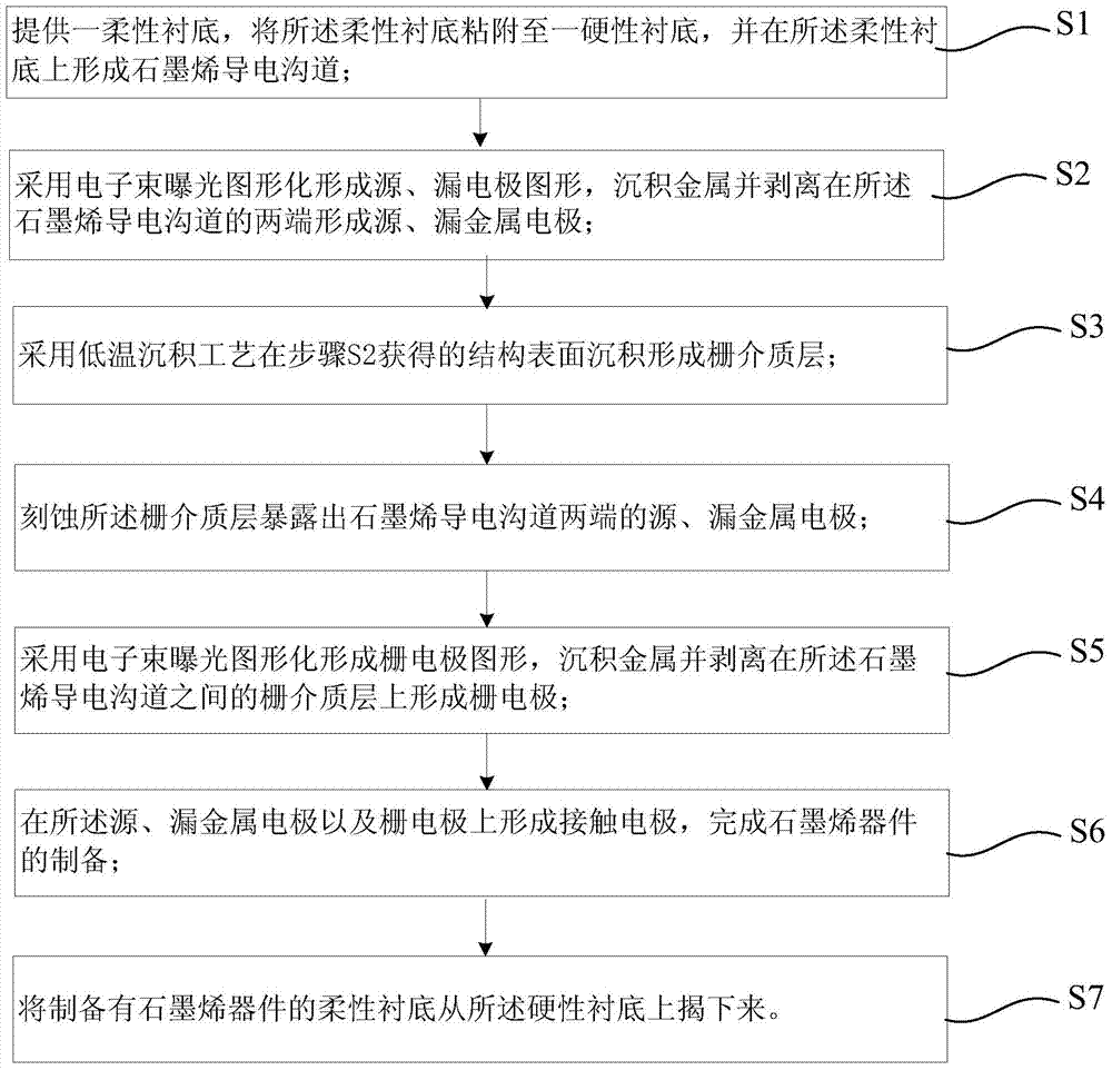
Method for preparing graphene device on flexible substrate
A flexible substrate, graphene technology, applied in the field of microelectronics
- Summary
- Abstract
- Description
- Claims
- Application Information
AI Technical Summary
Problems solved by technology
Method used
Image

Examples
specific Embodiment approach
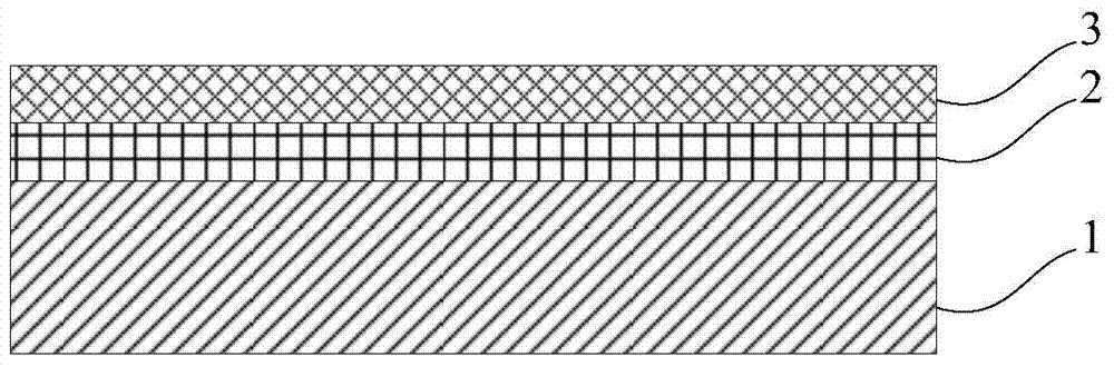
[0068] A double-layer e-beam photoresist is then coated on the substrate. The specific implementation is as follows: the upper surface of the flexible substrate 1 is spin-coated with PMMA1 type electron beam photoresist 2 (such as 495A5) by an automatic glue leveler, and the automatic glue leveler rotating speed is set to 500rpm at a slow speed first, and the time is 10s or so, and then fast 4000rpm, the time is about 45s, and then it can be dried at a temperature of about 180°C. Then spin-coat PMMA2 type electron beam photoresist 3 (such as 950A2), the speed is set to slow at 500rpm, the time is about 10s, and then fast at 4000rpm, the time is about 45s, and then the temperature is about 180 ℃ for drying . The obtained structure diagram is as follows figure 2 shown.
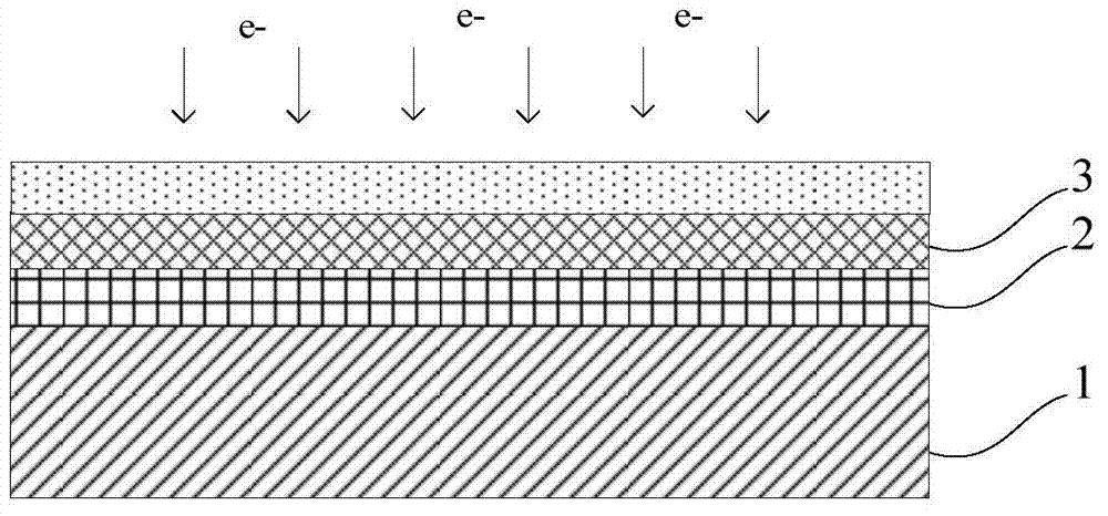
[0069] The electron beam photoresists PMMA1 and PMMA2 used are small molecular weight photoresists and large molecular weight photoresists respectively. After electron beam exposure photoresists, the long ca...
PUM
| Property | Measurement | Unit |
|---|---|---|
| thickness | aaaaa | aaaaa |
| thickness | aaaaa | aaaaa |
| thickness | aaaaa | aaaaa |
Abstract
Description
Claims
Application Information