Semiconductor device manufacturing method

A device manufacturing method and semiconductor technology, applied in semiconductor/solid-state device manufacturing, semiconductor devices, electrical components, etc., can solve problems such as corrosion, stress layer loss, DSL integration failure, etc., and achieve the effect of process integration

Active Publication Date: 2018-02-13
SOI MICRO CO LTD
View PDF3 Cites 0 Cited by
  • Summary
  • Abstract
  • Description
  • Claims
  • Application Information

AI Technical Summary

Problems solved by technology

In this case DSL integration failed due to stress layer loss
In addition, for the case where TEOS is deposited on the device, although the TEOS covering the stress layer after CMP will protect the stress layer from corrosion, the corrosion rate of TEOS in DHF is also relatively high, and the process of removing the dummy gate insulating layer During the process, TEOS is in danger of being completely corroded by DHF, which will expose the underlying tensile stress silicon nitride to the environment of DHF, resulting in the corrosion of tensile stress silicon nitride

Method used


Image

  • Semiconductor device manufacturing method
  • Semiconductor device manufacturing method
  • Semiconductor device manufacturing method

Examples


Embodiment Construction

[0028] Hereinafter, the present invention is described by means of specific embodiments shown in the drawings. It should be understood, however, that these descriptions are exemplary only and are not intended to limit the scope of the present invention. Also, in the following description, descriptions of well-known structures and techniques are omitted to avoid unnecessarily obscuring the concept of the present invention.

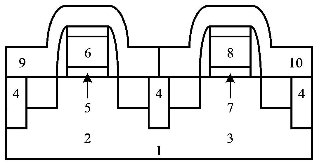
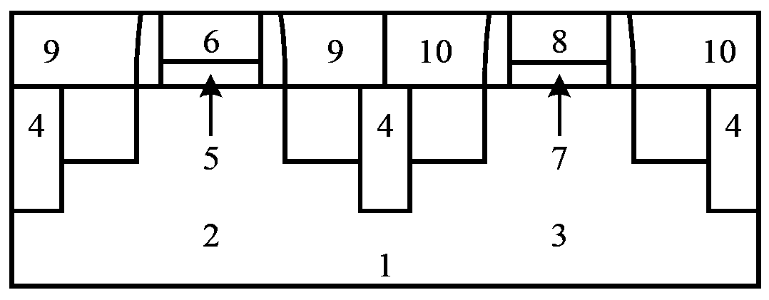
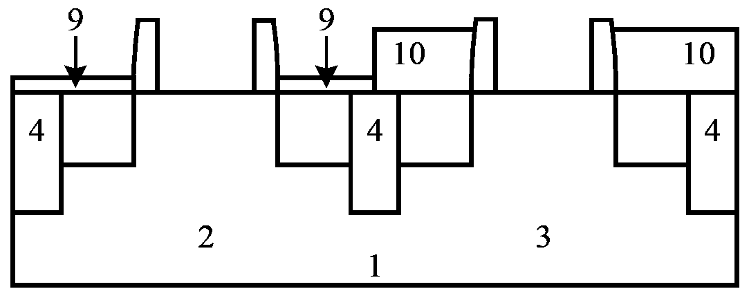
[0029] The present invention provides a method for manufacturing a semiconductor device, and in particular relates to a method for manufacturing a transistor using spacer technology. Please refer to the attached Figure 4-10 , the semiconductor device manufacturing method provided by the present invention will be described in detail.

[0030] First, see attached Figure 4 , on the semiconductor substrate 1 , NMOS 2 and PMOS 3 are formed, and different MOS transistors are isolated by STI structures 4 . Wherein, in this embodiment, a single crystal silicon...


PUM

PropertyMeasurementUnit
thicknessaaaaaaaaaa
thicknessaaaaaaaaaa
thicknessaaaaaaaaaa

Abstract

The invention provides a manufacturing method for a stress semiconductor device. In the method, firstly a tensile stress layer is deposited on an NMOS area so as to deposit a compressive stress layer on a PMOS area, and then a compressive stress protective layer is deposited comprehensively; through a first CMP process, dummy gates are opened and because the compressive stress protective layer of a part thickness is kept on the tensile stress layer and on the compressive stress layer and the corrosion rate of the compressive stress protective layers in a wet-process corrosive liquid is significantly low, the tensile stress layer and the compressive stress layer are protected by the compressive stress protective layers on the tensile stress layer and the compressive stress layer and free from damages when dummy-gate insulating layers are corroded and thus defects in the prior art are overcome; and next, after grid grooves are formed, a second CMP process can be performed selectively so as to remove the remaining compressive stress protective layers and then manufacturing of a high-K grid insulating layer and a metal gate is completed and integration of a gate last and a dual stressliner is realized.

Description

technical field [0001] The invention relates to the field of manufacturing methods of semiconductor devices, in particular to an integration method of a double strain stress layer applied in a CMOS gate-last process. Background technique [0002] After semiconductor integrated circuit technology enters the technology node of 90nm feature size, it becomes more and more challenging to maintain or improve transistor performance. After the 90nm node, stress technology is gradually adopted to improve device performance. At the same time, in terms of manufacturing process, the high-K metal gate technology in the gate last process (gate last) is also gradually adopted to meet the challenges brought about by the continuous reduction of devices. In the stress technology, the dual stress layer (DSL, dual stressliner) technology has high compatibility with conventional processes and low cost, so it is adopted by major semiconductor manufacturers. [0003] DSL technology refers to the...

Claims


Application Information

Patent Timeline
Patent Type & Authority Patents(China)
IPC IPC(8): H01L21/8238
CPCH01L21/823828H01L21/823857H01L29/7843
Inventor 秦长亮尹海洲殷华湘
Owner SOI MICRO CO LTD
Why Eureka
Try Eureka