Photonic crystal laser array with high brightness and horizontal far-field single distribution

A technology of laser arrays and photonic crystals, applied in semiconductor laser devices, laser devices, etc., can solve problems such as large divergence angles, and achieve the effects of easy integration, simple preparation process, and simple process

Active Publication Date: 2015-06-10
INST OF SEMICONDUCTORS - CHINESE ACAD OF SCI
View PDF3 Cites 0 Cited by
  • Summary
  • Abstract
  • Description
  • Claims
  • Application Information

AI Technical Summary

Problems solved by technology

[0005] In view of this, the main purpose of the present invention is to provide a photonic crystal laser array that realizes high-brightness level far-field single-lobe distribution, and solve the problem that the output far field of the edge-emitting laser array is double-lobed and the divergence angle is limited by the function of photonic crystal modulation phase. Big problem, to achieve the purpose of outputting high-brightness single-lobe far-field laser

Method used


Image

  • Photonic crystal laser array with high brightness and horizontal far-field single distribution
  • Photonic crystal laser array with high brightness and horizontal far-field single distribution
  • Photonic crystal laser array with high brightness and horizontal far-field single distribution

Examples


Embodiment

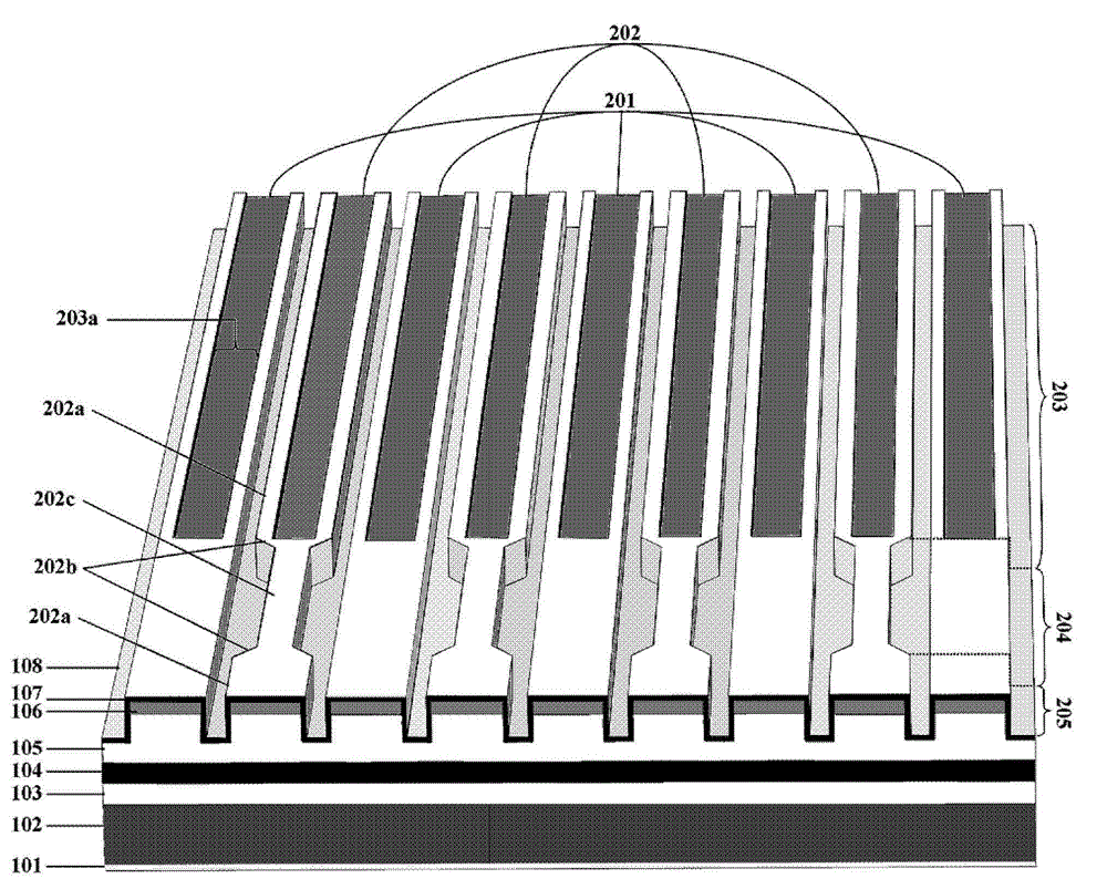
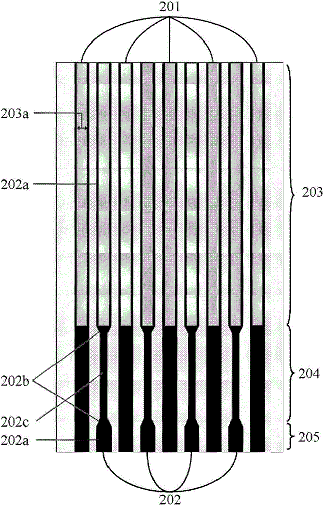
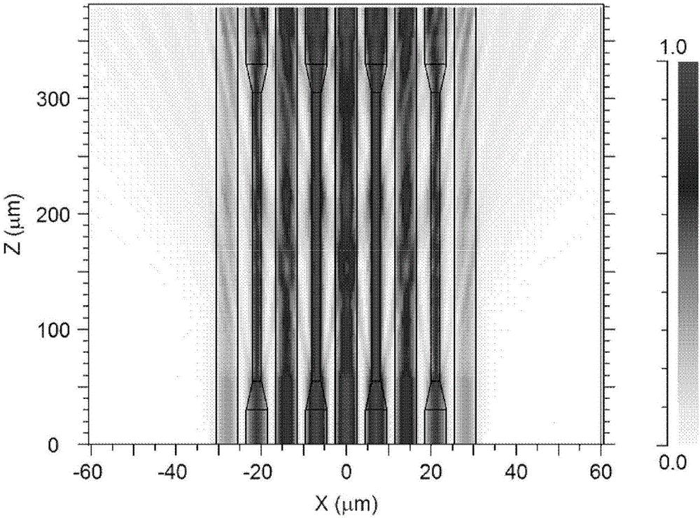
[0043] figure 2 It is a schematic diagram of the surface geometric structure of an embodiment of a photonic crystal laser array that realizes a high-brightness horizontal far-field single lobe distribution. As shown in the figure, the array of this embodiment includes 9 waveguides. In the mode coupling region 203, the width of each waveguide is 5 μm, the width of the region between adjacent waveguides is 2 μm, and the length of the entire coupling region is 1000 μm. In the photonic crystal region 204, the width of the first strip waveguide 201 is still 5 μm, and the width of the third strip waveguide 202c is 2 μm. The length of the entire photonic crystal region is 300 μm, the length of the two tapered waveguides 202b is 25 μm, and the length of the third strip waveguide 202c is 250 μm. The width of all the waveguides in the emission area 205 is 5 μm, and the length of the waveguides is 100 μm. The waveguide in the whole area is realized by a one-step etching process, and the...


PUM


Abstract

The invention relates to the technical field of semiconductor photoelectronic devices, and discloses a photonic crystal laser array with high brightness and horizontal far-field single distribution. According to the photonic crystal laser array, phase modulation of the laser array output mode is carried out through photonic crystal, and laser output with high brightness and horizontal far-field single distribution is generated. The photonic crystal laser array comprises a module coupling area, a photonic crystal area and a transmission area, wherein the mode coupling area generates a stable opposite-phase mode which is modulated by the photonic crystal area and is converted into a same-phase distribution mode, and the converted mode outputs a single far-field pattern with a narrow divergence angle on the reflection area. The waveguides of the module coupling area, the photonic crystal area and the transmission area are all completed through traditional ordinary photoetching and etching processes. The photonic crystal laser array with high brightness and horizontal far-field single distribution effectively solves the problem that when the output power of a semiconductor transmission laser array is too high, horizontal far-field double distribution and a large divergence angle occur, and generates high-brightness laser, and the brightness of the laser is improved by one level expectedly.

Description

Technical field [0001] The invention relates to the technical field of semiconductor optoelectronic devices, in particular to a photonic crystal laser array that realizes high-brightness level far-field single lobe distribution. Background technique [0002] Semiconductor lasers have high electro-optical conversion efficiency, and have the advantages of wide coverage, long life, direct modulation, small size, and low cost. Among them, the edge-emitting semiconductor laser array has great advantages in terms of high efficiency and high power laser output. The continuous output power of a single laser bar at room temperature has exceeded one hundred watts, and the output power of laser stacks has also exceeded kilowatts. However, the far-field characteristics in the horizontal direction (direction parallel to the pn junction plane) are not good, generally showing a double-lobe distribution with a large far-field divergence angle, which reduces the brightness of the laser. This gre...

Claims


Application Information

Patent Timeline
Patent Type & Authority Patents(China)
IPC IPC(8): H01S5/40
Inventor 郑婉华刘磊张建心渠红伟
Owner INST OF SEMICONDUCTORS - CHINESE ACAD OF SCI
Why Eureka
Try Eureka