Photonic crystal laser array with high brightness and horizontal far-field single distribution
A technology of laser arrays and photonic crystals, applied in semiconductor laser devices, laser devices, etc., can solve problems such as large divergence angles, and achieve the effects of easy integration, simple preparation process, and simple process
- Summary
- Abstract
- Description
- Claims
- Application Information
AI Technical Summary
Problems solved by technology
Method used
Image
Examples
Embodiment
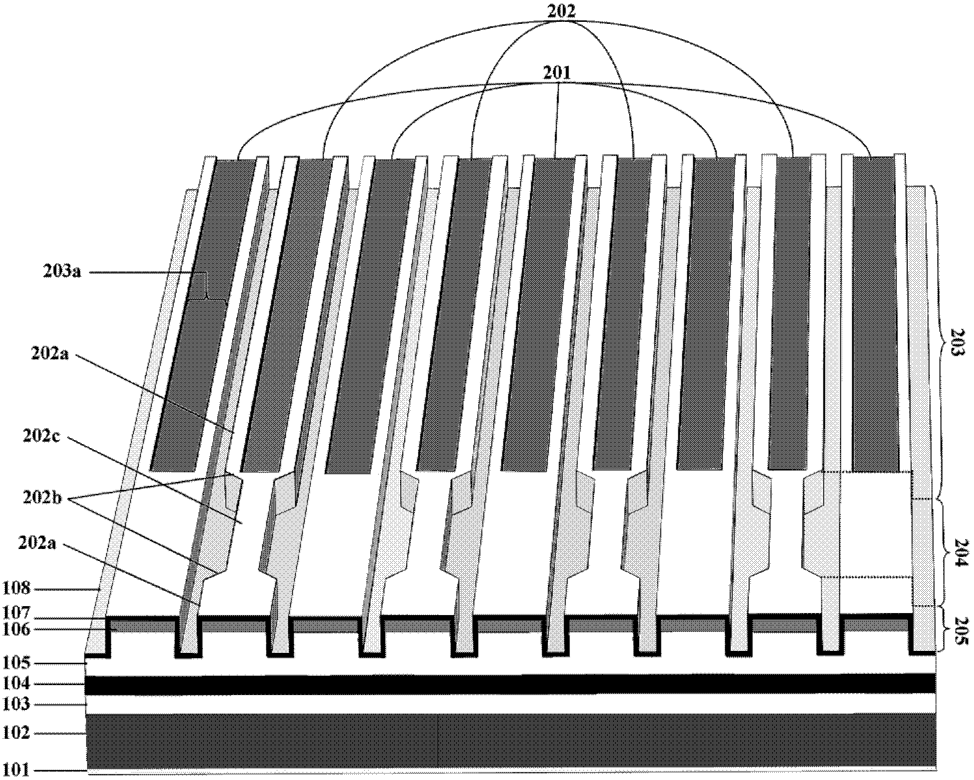
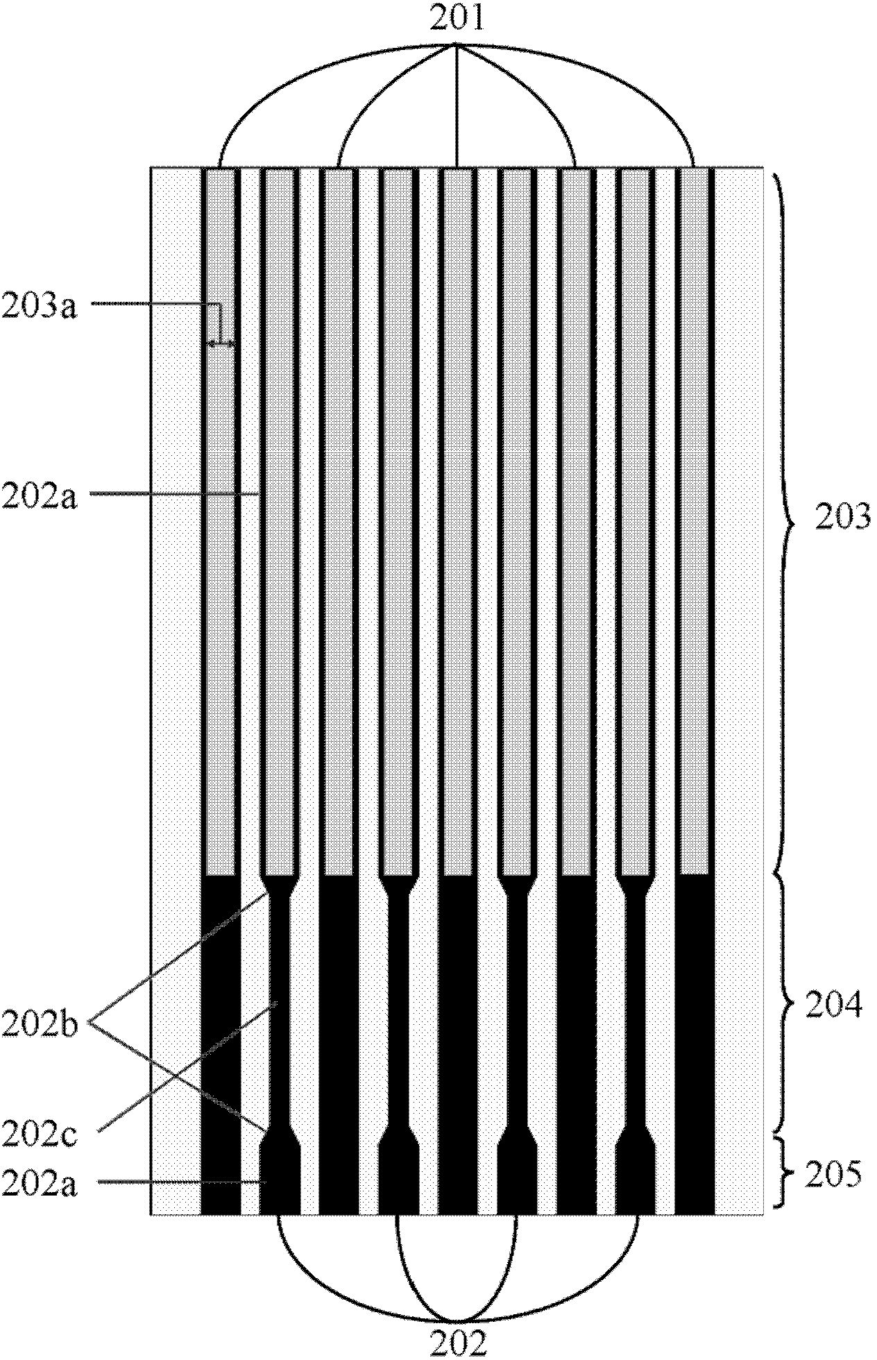
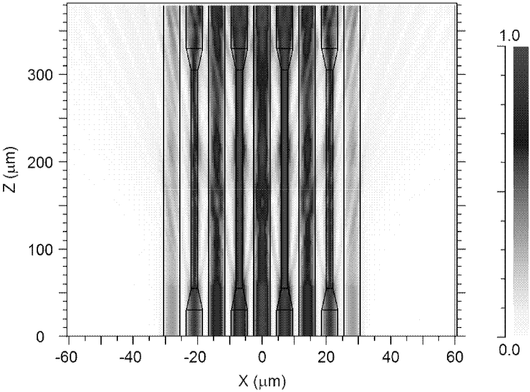
[0043] figure 2 It is a schematic diagram of the surface geometric structure of an embodiment of a photonic crystal laser array that realizes high-brightness level far-field single-lobe distribution. As shown in the figure, the array of this embodiment includes 9 waveguides. In the mode coupling region 203, the width of each waveguide is 5 μm, the width of the region between adjacent waveguides is 2 μm, and the length of the entire coupling region is 1000 μm. In the photonic crystal region 204, the width of the first strip waveguide 201 is still 5 μm, and the width of the third strip waveguide 202c is 2 μm. The length of the entire photonic crystal region is 300 μm, the length of the two tapered waveguides 202 b is 25 μm, and the length of the third strip waveguide 202 c is 250 μm. All the waveguides in the emission area 205 have a width of 5 μm and a waveguide length of 100 μm. The waveguide in the whole area is realized by one-step etching process, and the etching depth i...
PUM
 Abstract
Description
Claims
Application Information


