Supercharge Your Innovation With Domain-Expert AI Agents!

Distributed building blocks for r-c clamp circuits in the core region of a semiconductor die

A core area, clamping circuit technology, applied in semiconductor devices, circuits, transistors, etc., can solve problems such as occupying chips and restricting wiring options

Active Publication Date: 2016-08-31
QUALCOMM INC
View PDF3 Cites 0 Cited by
  • Summary
  • Abstract
  • Description
  • Claims
  • Application Information

AI Technical Summary

Problems solved by technology

Each of these designs consumes a large portion of the chip's metal layers, greatly constraining routing options for the chip's other functional components

Method used


Image

  • Distributed building blocks for r-c clamp circuits in the core region of a semiconductor die
  • Distributed building blocks for r-c clamp circuits in the core region of a semiconductor die
  • Distributed building blocks for r-c clamp circuits in the core region of a semiconductor die

Examples


Embodiment Construction

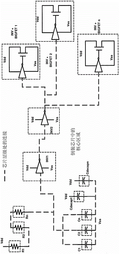
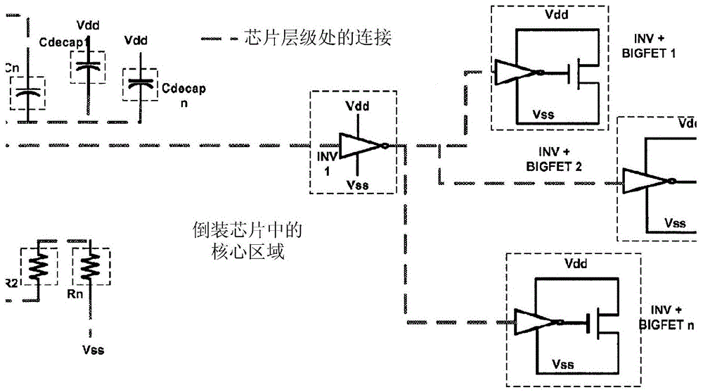
[0013] One disadvantage of conventional timer-based clamp circuit designs is that the timer-based clamp occupies a large area and it uses a large portion of the conductive (eg, metal) layer to handle the ESD current. This introduces a problem at the block or chip level, since a considerable area is allocated to place the timer-based (e.g., RC) clamp, resulting in congestion due to conductive layer congestion within the timer-based clamp. Increases the difficulty of routing signals in the core area.

[0014] According to aspects of the present invention, these problems with conventional timer-based clamper implementations can be mitigated by distributing the building blocks of the timer-based clamper. Distributed timer-based clamps can be applied in a flip-chip configuration or any other chip configuration.

[0015] Figure 1A is a block diagram of an exemplary timer-based clamp circuit in which components of the timer-based circuit (eg, resistors and capacitors) are distribut...


PUM


Abstract

A semiconductor die includes a resistor-capacitor RC clamp circuit for electrostatic discharge (ESD) protection of the semiconductor die. The RC clamp circuit includes building blocks distributed in a pad ring and in a core area of ​​the semiconductor die. The building blocks include at least one capacitor block in the core region. The RC clamp circuit also includes chip level conductive layer connections between each of the distributed building blocks.

Description

technical field [0001] The present invention relates generally to semiconductor circuits that provide protection against potentially damaging excessive voltages, including, by way of example, excessive electrical overstress (EOS) and / or electrostatic discharge (ESD) events. Voltage. Background technique [0002] Modern integrated circuits (ICs) are susceptible to damage from excess voltage. Common sources of these potentially damaging voltages include electrical overstress (EOS) and electrostatic discharge (ESD). ESD, a serious problem in solid-state electronic devices, is the transfer of electrostatic charges between bodies or surfaces at different electrostatic potentials, either through direct contact or through induced electric fields. ICs constructed using semiconductors, such as silicon, and insulating materials, such as silicon dioxide, can be permanently damaged when subjected to higher voltages that can be generated by an ESD event. [0003] Traditionally, on-chi...

Claims


Application Information

Patent Timeline
Patent Type & Authority Patents(China)
IPC IPC(8): H01L27/02
CPCH01L27/0285H01L27/0296H01L2924/0002H01L2924/00Y10T29/4913
Inventor 礼萨·贾利利塞纳里埃文·希安苏里斯雷克尔·R·敦迪盖尔尤金·R·沃利
Owner QUALCOMM INC
Features
  • R&D
  • Intellectual Property
  • Life Sciences
  • Materials
  • Tech Scout
  • Unparalleled Data Quality
  • Higher Quality Content
  • 60% Fewer Hallucinations
Learn More