Circuit laminated board structure
A technology of circuit layer and laminated board, applied in the direction of printed circuit components, etc., can solve problems such as bending, failure, short circuit, etc.
- Summary
- Abstract
- Description
- Claims
- Application Information
AI Technical Summary
Problems solved by technology
Method used
Image
Examples
Embodiment Construction
[0027] The implementation of the present invention will be described in more detail in conjunction with the drawings and component symbols below, so that those skilled in the art can implement it after studying this specification.
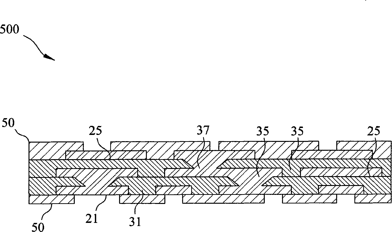
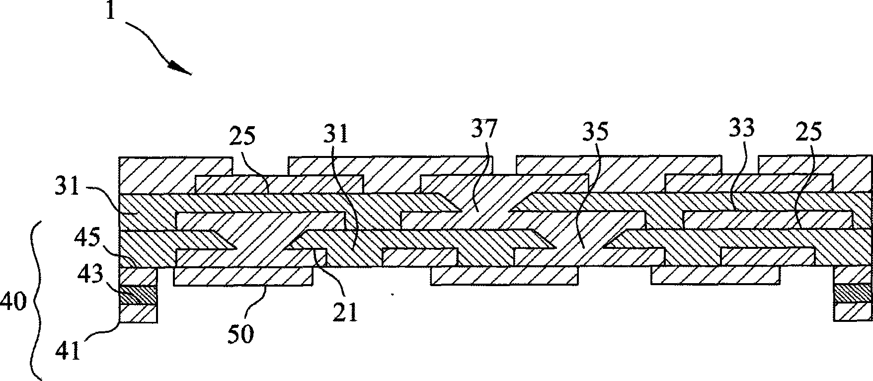
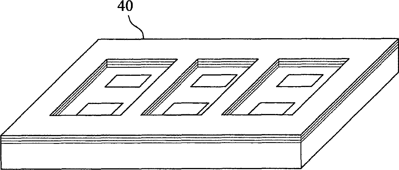
[0028] refer to Figure 2A , is a schematic cross-sectional view of the circuit laminate structure of the present invention. As shown in Figure 2, the circuit laminate structure 1 of the present invention comprises a first circuit layer 21, a first insulating layer 31, at least one second circuit layer 25, at least one second insulating layer 33, a supporting frame 40 and A solder resist layer 50, and the total thickness of the circuit laminate structure 1 is less than 150um.
[0029] The first insulating layer 31 is disposed on the first wiring layer 21, covers the upper surface of the first wiring layer 21, and forms a coplanar surface with the lower surface of the first wiring layer 21, and on the coplanar surface, Part of the first circuit la...
PUM
 Abstract
Description
Claims
Application Information


