Method for monitoring edge thickness measurement stability of wafer
A technology of edge thickness and stability, applied in the field of wafer edge thickness measurement stability monitoring, can solve problems such as the inability to reflect the stability of wafer edge thickness
- Summary
- Abstract
- Description
- Claims
- Application Information
AI Technical Summary
Problems solved by technology
Method used
Image

Examples
Embodiment Construction
[0022] In order to make the content of the present invention clearer and easier to understand, the content of the present invention will be described in detail below in conjunction with specific embodiments and accompanying drawings.
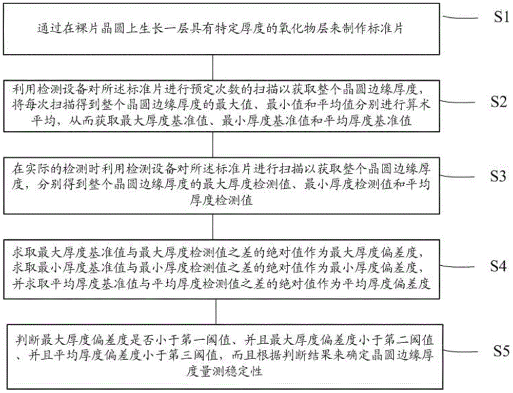
[0023] The principle of the invention is to use a layer of oxide grown on a bare wafer as a standard wafer for machine testing. Then scan multiple times continuously on the detection equipment, and carry out arithmetic average of the maximum, minimum and average values of the edge thickness of the entire wafer obtained by each scan, and use the calculated arithmetic average value and this wafer as the indicator of thickness measurement stability standard value. In the actual detection, use the detection equipment to scan the standard sheet, obtain the maximum value, minimum value and average value of the edge thickness of the entire wafer respectively and compare them with the standard value, and use the difference to determine the deviation o...
PUM
 Abstract
Description
Claims
Application Information
 - R&D
- Intellectual Property
- Life Sciences
- Materials
- Tech Scout
- Unparalleled Data Quality
- Higher Quality Content
- 60% Fewer Hallucinations
Browse by: Latest US Patents, China's latest patents, Technical Efficacy Thesaurus, Application Domain, Technology Topic, Popular Technical Reports.
© 2025 PatSnap. All rights reserved.Legal|Privacy policy|Modern Slavery Act Transparency Statement|Sitemap|About US| Contact US: help@patsnap.com