Touch-sensing electrode structure and touch-sensitive device

A technology of touch sensing and electrode structure, applied in electrical components, electronic switches, electrical digital data processing, etc., can solve problems such as high line impedance, excessive bonding area, and large number of channels, and achieve improved touch linearity , Improve sensitivity, reduce the number of channels and the effect of line impedance

Inactive Publication Date: 2014-03-12
WINTEK CORP
View PDF5 Cites 25 Cited by
  • Summary
  • Abstract
  • Description
  • Claims
  • Application Information

AI Technical Summary

Problems solved by technology

Furthermore, the number of channels required by the single-layer ITO structure is very large, which will lead to high line impedance, and the X-axis and Y-axis sensing electrodes are likely to form an excessively large bonding area on a flexible circuit board.

Method used


Image

  • Touch-sensing electrode structure and touch-sensitive device
  • Touch-sensing electrode structure and touch-sensitive device
  • Touch-sensing electrode structure and touch-sensitive device

Examples


Embodiment Construction

[0055] The aforementioned and other technical contents, features and effects of the present invention will be clearly presented in the following detailed description of the embodiments with reference to the drawings. The directional terms mentioned in the following embodiments, such as: up, down, left, right, front or back, etc., are only directions referring to the attached drawings. Accordingly, the directional terms used are illustrative and not limiting of the invention.

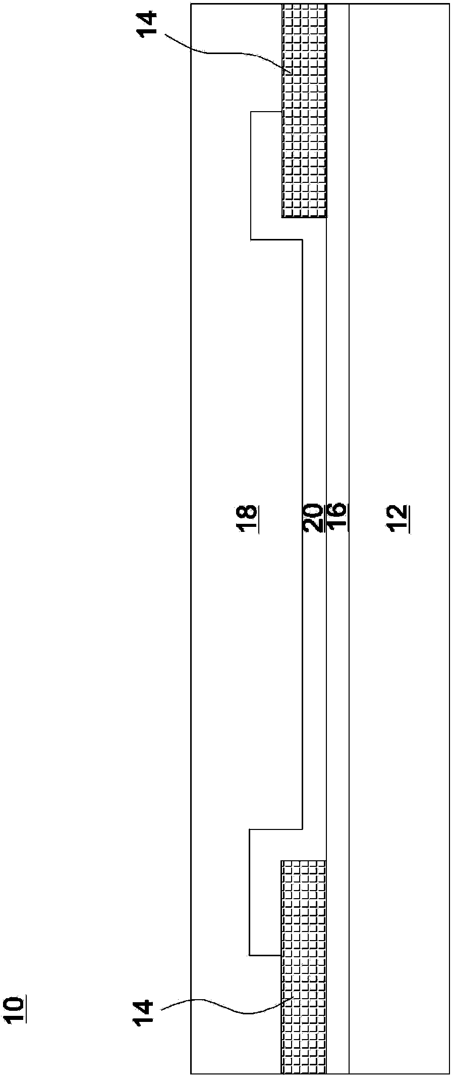
[0056] figure 1 It is a schematic diagram of a touch device according to an embodiment of the present invention. Such as figure 1As shown, in a touch device 10 , a touch sensing electrode structure 20 is disposed on a substrate 12 . The substrate 12 can be, for example, a cover lens or a substrate of a display. For example, the substrate 12 can be used as a color filter substrate, an array substrate (array sinstrate), or a packaging cover for an organic light-emitting display (OLED), so that the touch...


PUM


Abstract

A touch-sensing electrode structure includes multiple first electrodes and multiple second electrodes. Each first electrode includes a longitudinal part extending in a first direction and multiple branch parts connected to the longitudinal part. The second electrodes are disposed on at least one side of each longitudinal part, and each of the second electrodes at least spreads over a region between two adjacent branch parts of each of the first electrodes. Through the invention, the inductive capacitance of the touch-sensing electrode structure and the sensitivity of the touch control operation can be improved, and the effect of touch-sensing linearity can be improved, and channels required by a single-layer touch-sensing structure and line impdedance can be reduced.

Description

technical field [0001] The invention relates to a touch sensing electrode structure and a touch device. Background technique [0002] At present, the touch sensing electrode structure of the capacitive touch device is usually formed by double-side ITO (double-side ITO) or single-side ITO (single-side ITO) process. In a double-sided ITO process, it is necessary to perform coating and lithographic etching processes on both sides of the glass substrate to form X-axis and Y-axis sensing electrodes on both sides of the glass substrate. It is easy to cause the yield rate to drop. In addition, in a single-sided ITO process, the X-axis and Y-axis sensing electrodes are formed on the same side of the glass substrate. Due to the need for cross-bridge structure design in the plane, the X-axis and Y-axis sensing electrodes are prone to instability due to the material properties of the organic insulating layer. or other factors causing short circuit or open circuit problems. Therefore...

Claims


Application Information

Patent Timeline
Patent Type & Authority Applications(China)
IPC IPC(8): G06F3/041G06F3/044
CPCH03K2017/9602G06F3/044H03K2217/960755H03K17/9622H03K2217/960785G06F3/04164G06F3/0443G06F3/0448
Inventor 张廷宇廖小惠何昆璋吴法震李广为苏国彰
Owner WINTEK CORP
Why Eureka
Try Eureka