
Method for controlling wafer cooling in semiconductor process
A technology for controlling wafers and semiconductors, applied in semiconductor/solid-state device manufacturing, electrical components, circuits, etc., can solve problems such as adjusting cooling conditions, excessive nitrogen consumption, and low cooling efficiency, and achieve nitrogen resource conservation, control and shortening, The effect of increasing productivity
- Summary
- Abstract
- Description
- Claims
- Application Information
AI Technical Summary
Problems solved by technology
Method used
Image

Examples
Embodiment 1
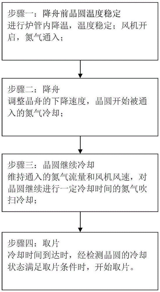
[0032] In this example, see figure 1 . figure 1 It is a flowchart of a method for controlling wafer cooling in a semiconductor process of the present invention. As shown in the figure, the method for controlling wafer cooling of the present invention is aimed at oxidation, low-pressure chemical vapor deposition or The low-temperature annealing process is implemented, including four steps of stabilizing the wafer temperature before lowering the boat, lowering the boat, continuing to cool the wafer, and picking up the wafer, as follows:
[0033] Step 1: The temperature of the wafer is stabilized before landing the boat. In the cooling stage of the furnace tube of the semiconductor process, according to the different types of processes, the temperature in the furnace tube is lowered to a temperature range of different heights and stabilized; and, according to the different requirements for oxygen content of different types of processes, the vertical The flow of nitrogen gas use...
Embodiment 2
[0054] In this embodiment, for the oxidation process, the following relevant cooling control parameters are set and implemented:
[0055] (1) The temperature of the wafer is stabilized before the boat is lowered: before the boat is lowered, the temperature is stabilized, and the temperature in the furnace tube is lowered to 600°C to stabilize; the number of wafers in a batch is 125, and the size of the wafer is 300mm;
[0056] (2) The fan is turned on: the wind speed is 0.3m / s, which can form a relatively stable laminar airflow;
[0057] (3) For the vertical furnace oxidation process, the requirements for the oxygen content in the load-bearing area are not high, and air is introduced into the load-bearing area instead of nitrogen for purging and cooling. The air flow rate is 300slm; 200mm / min;
[0058] (4) Continue cooling of the wafer: under nitrogen purge, the cooling time of the wafer in the loading area is 25 minutes, and the temperature of the wafer has reached below 50°...
Embodiment 3
[0061] In this embodiment, for the low-pressure chemical vapor deposition process, the following relevant cooling control parameters are set and implemented:
[0062] (1) The temperature of the wafer is stabilized before the boat is lowered: before the boat is lowered, the temperature is stabilized, the temperature in the furnace tube is lowered to 500°C to stabilize, and the pressure is returned to normal pressure; the number of wafers in a batch is 125 pieces, and the specifications of the wafer The size is 300mm;
[0063] (2) The fan is turned on: the wind speed is 0.4m / s, which can form a relatively stable laminar airflow;
[0064] (3) For the vertical furnace low-pressure chemical vapor deposition process, the oxygen content in the load-bearing area is required to be relatively high, requiring <5ppm, and the flow rate of nitrogen gas is 800slm, which not only ensures the cooling effect of the wafer, but also ensures the oxygen content in the load-bearing area. The conten...
PUM
 Abstract
Description
Claims
Application Information