Sub pixel-based 3D integrated imaging display device
A display device, integrated imaging technology, applied in the field of 3D display
- Summary
- Abstract
- Description
- Claims
- Application Information
AI Technical Summary
Problems solved by technology
Method used
Image
Examples
Embodiment Construction
[0031] Embodiments of the present invention will now be described in detail, examples of which are illustrated in the accompanying drawings, wherein like reference numerals refer to like parts throughout. The embodiments are described below in order to explain the present invention by referring to the figures.
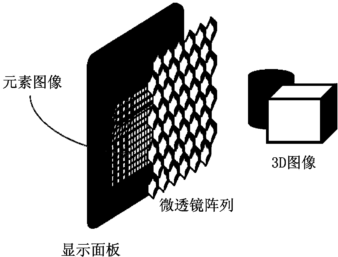
[0032] figure 1 is a diagram illustrating the structure of a subpixel-based 3D integrated imaging display device according to an embodiment of the present invention.
[0033] like figure 1 As shown, the subpixel-based 3D integrated imaging display device according to the present invention includes a common 2D thin display panel and a microlens array, wherein the microlens array covers the common 2D thin display panel and the microlens array is arranged on the output side of the display panel .
[0034] The general 2D thin display panel may be a matrix display panel having an array of display elements arranged in rows and columns, and each display element generates a...
PUM
 Abstract
Description
Claims
Application Information


