Unit mask, mask assembly and method of manufacturing organic light emitting diode display

A mask assembly and mask technology, applied in semiconductor/solid-state device manufacturing, printed circuit manufacturing, electroluminescent light sources, etc., can solve problems such as unit mask deformation, and achieve the effect of improving deposition reliability.

Active Publication Date: 2017-06-20
SAMSUNG DISPLAY CO LTD
View PDF6 Cites 0 Cited by
  • Summary
  • Abstract
  • Description
  • Claims
  • Application Information

AI Technical Summary

Problems solved by technology

[0006] However, when the unit mask becomes very thin, it becomes difficult to weld both ends of the unit mask to the frame to fix the unit mask to the frame
[0007] Also, when the unit mask is very thin, since both ends of the unit mask are extended and fixed to the frame, the unit mask may sag through the opening, or the unit mask may be deformed by tension applied to the unit mask.

Method used


Image

  • Unit mask, mask assembly and method of manufacturing organic light emitting diode display
  • Unit mask, mask assembly and method of manufacturing organic light emitting diode display
  • Unit mask, mask assembly and method of manufacturing organic light emitting diode display

Examples


Embodiment Construction

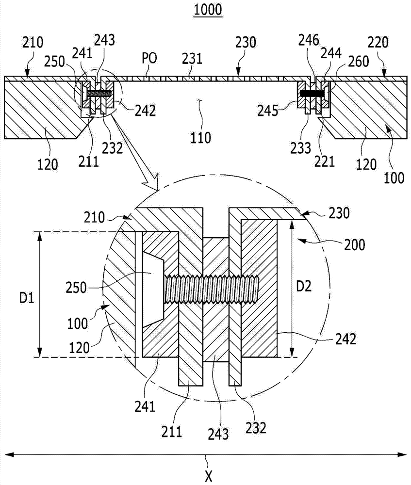
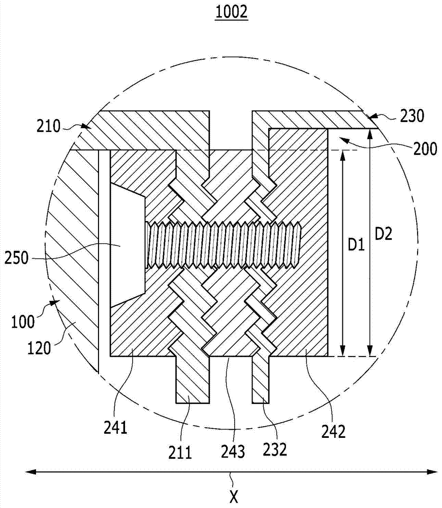
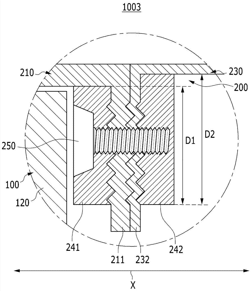
[0032] The present invention will be described more fully hereinafter with reference to the accompanying drawings, in which certain embodiments of the invention are shown. As those skilled in the art would realize, the described embodiments may be modified in various ways, all without departing from the spirit or scope of the present invention.

[0033] The drawings and descriptions are to be regarded as illustrative in nature and not restrictive. Like numbers generally refer to like elements throughout the specification.

[0034] Throughout the disclosed embodiments, the same reference numerals will be used to refer to the same or similar components. The first embodiment will be described as a representative embodiment, and only parts of the other embodiments that are different from the first embodiment will be described.

[0035] In the drawings, the size and thickness of components may be exaggerated, omitted, or schematically shown for clarity and convenience of descript...


PUM


Abstract

The invention provides a unit mask, a mask component and a method for manufacturing an organic light emitting diode display. The unit mask extends in one direction and is supported by a frame including openings. The unit mask includes: a first fixing part positioned in the opening and fixed to one surface of the frame disposed along the one direction; a second fixing part spaced apart from the first fixing part and fixed to the frame disposed along the one direction. The other surface of the frame; and the mask part held between the first fixing part and the second fixing part by the first fixing part and the second fixing part.

Description

technical field [0001] The described techniques generally involve a unit mask supported by a frame and a mask assembly. Background technique [0002] Examples of flat panel displays include organic light emitting diode (OLED) displays, liquid crystal displays (LCD), and plasma display panels (PDP). [0003] In order to manufacture an OLED display, it is generally necessary to form electrodes in a specific pattern and form an emission layer. The electrodes and the emission layer may be formed using a deposition method using a mask assembly. [0004] A conventional mask assembly generally includes a frame having an opening and a plurality of unit masks in a stripe shape. Both ends of each unit mask extend corresponding to the opening and are fixed to the frame. The unit mask may include patterned openings corresponding to pixels of the OLED display, so that the OLED display may be fabricated on the mother substrate. The patterned openings of each unit mask may correspond t...

Claims


Application Information

Patent Timeline
Patent Type & Authority Patents(China)
IPC IPC(8): H01L51/56
CPCC23C14/042H10K71/166H10K71/00H05B33/10H05K3/184H05K3/1225B05C17/08B05C21/005
Inventor 李相信
Owner SAMSUNG DISPLAY CO LTD
Why Eureka
Try Eureka