Shift register unit, shift register and display device

A shift register, reset signal technology, applied in static memory, digital memory information, instruments, etc., can solve the problems of inability to reduce integrated circuit power consumption, abnormal reset signal waveform, etc., to reduce the connection time and reduce the power consumption. consumption effect

Active Publication Date: 2017-07-28
BEIJING BOE OPTOELECTRONCIS TECH CO LTD
View PDF6 Cites 0 Cited by
  • Summary
  • Abstract
  • Description
  • Claims
  • Application Information

AI Technical Summary

Problems solved by technology

However, the output of each stage of the shift register unit in the above shift register is used as the reset signal of the previous row of shift register units, so as the shift registers are cascaded, there will be a problem that the waveform of the reset signal is abnormal; and , since the first clock signal or the second clock signal and the output terminal are kept in a conduction state during the high level period, the power consumption of the integrated circuit cannot be reduced

Method used


Image

  • Shift register unit, shift register and display device
  • Shift register unit, shift register and display device
  • Shift register unit, shift register and display device

Examples


Embodiment Construction

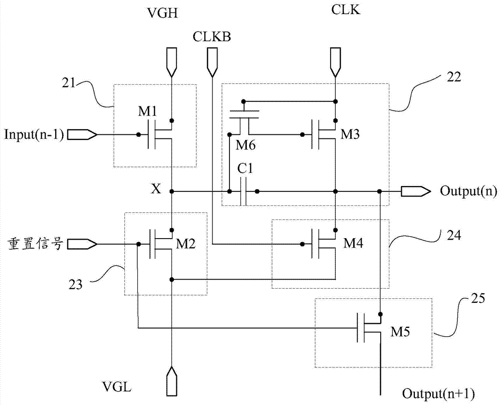
[0035] The following will clearly and completely describe the technical solutions in the embodiments of the present invention with reference to the drawings in the embodiments of the present invention. The transistors used in all the embodiments of the present invention can be field effect transistors. Since the source and drain of the field effect transistors used here are symmetrical, there is no difference between their source and drain. In the embodiment of the present invention, in order to distinguish the two poles of the field effect transistor except the gate, the first pole is called the source, and the second pole is called the drain. According to the form in the accompanying drawings, the upper end of the field effect transistor is defined as the source, and the lower end is the drain.

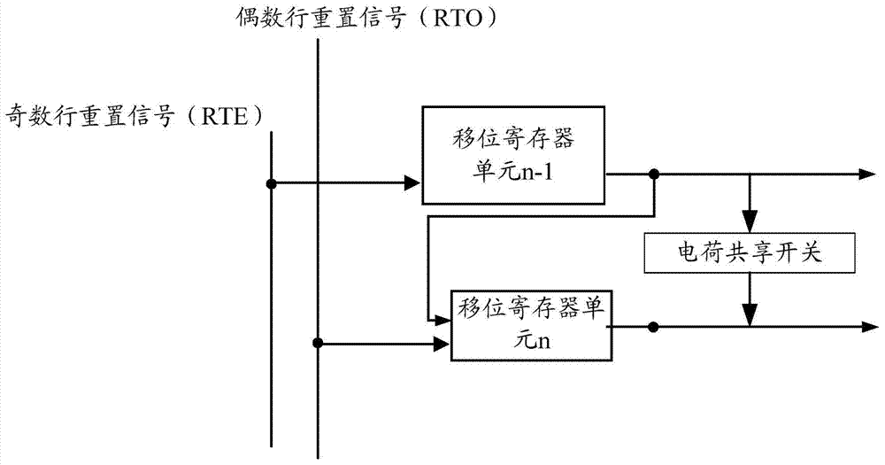
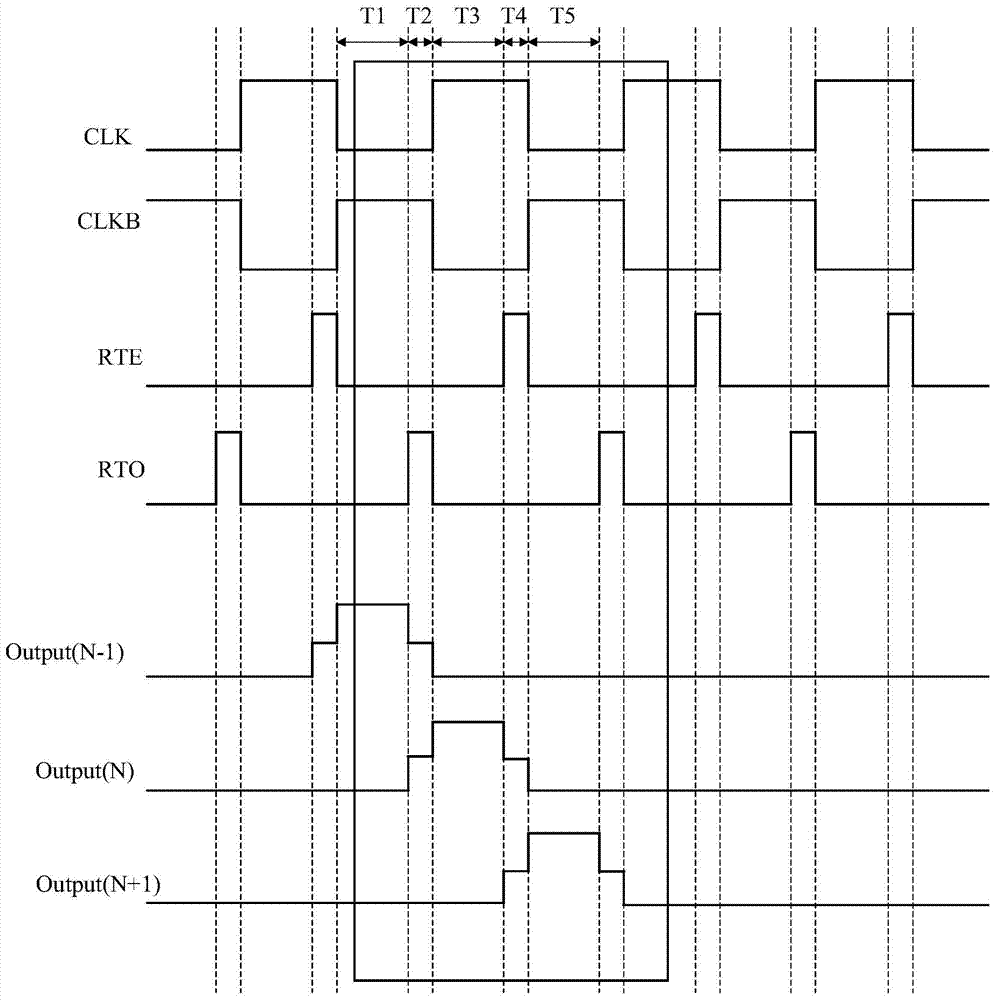
[0036] A kind of shift register provided by the embodiment of the present invention, such as figure 1 The illustration includes at least two shift register units; where the gate dr...


PUM


Abstract

The invention discloses a shift register unit, a shift register and a display device. The shift register unit includes: a voltage boosting module, which is used to , output the first level signal to the signal output module; the signal output module is used to output the gate drive signal under the control of the first clock signal according to the first level signal; the reset module is used to reset the signal Under the control of the control signal output module reset; the pull-down module is used to pull down the output level of the signal output module under the control of the second clock signal. The invention can reduce the power consumption of the integrated circuit and avoid the problem of abnormal waveform caused by the attenuation of the reset signal.

Description

technical field [0001] The invention relates to the field of display technology, in particular to a shift register unit, a shift register and a display device. Background technique [0002] At present, the shift register can integrate the gate (Gate) switch circuit on the array substrate, remove the circuit of the gate drive integrated circuit, and use the shift register to integrate the array substrate. The display composed of the array substrate can save materials and Process steps are reduced, and screen size and product cost are reduced. [0003] The above-mentioned shift register has a plurality of shift register units, and each shift register unit has input terminals such as a first clock signal, a second clock signal and a low voltage signal, and each shift register unit also has an input terminal (Input ), the output terminal (Output) and the reset signal (Reset). However, the output of each stage of the shift register unit in the above shift register is used as th...

Claims


Application Information

Patent Timeline
Patent Type & Authority Patents(China)
IPC IPC(8): G11C19/28G09G3/20
CPCG11C19/28G09G2310/0286G09G2300/0426G09G2310/08G09G2330/021
Inventor 王智勇于尧徐帅张郑欣郑义
Owner BEIJING BOE OPTOELECTRONCIS TECH CO LTD
Why Eureka
Try Eureka