Transparent substrates apparatus with locating structure and assembling method thereof

A transparent substrate and positioning structure technology, applied in the direction of identification devices, instruments, etc., can solve the problem of uneven gap between the transparent substrate and the shell

Active Publication Date: 2015-05-27
WISTRON CORP
View PDF5 Cites 1 Cited by
  • Summary
  • Abstract
  • Description
  • Claims
  • Application Information

AI Technical Summary

Problems solved by technology

[0005] The purpose of the present invention is to provide a transparent substrate with a positioning structure and an assembly method thereof. At least two positioning structures are arranged on the transparent substrate. When the transparent substrate is assembled in a casing of an electronic device, the two positioning structures of the transparent substrate Directly assembled on at least two positionin

Method used


Image

  • Transparent substrates apparatus with locating structure and assembling method thereof
  • Transparent substrates apparatus with locating structure and assembling method thereof
  • Transparent substrates apparatus with locating structure and assembling method thereof

Examples


Embodiment Construction

[0044] In order to enable your review committee members to have a further understanding and understanding of the characteristics of the present invention and the achieved effects, I would like to provide various embodiments and detailed descriptions, as follows:

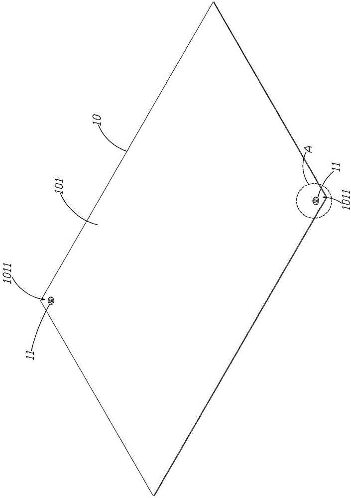
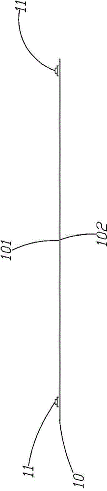
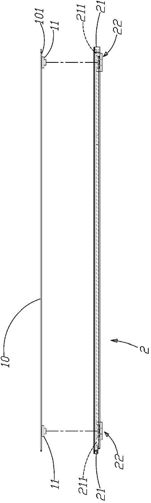
[0045] It is known that when a transparent substrate is to be assembled on a housing of an electronic device, the assembler visually adjusts the gap between the transparent substrate and the housing, but the gap between the transparent substrate and the housing is likely to be uneven, so that the assembler needs to The position of the transparent substrate is readjusted, so it takes more assembly time. In view of the above problems, the present invention provides a transparent substrate with a positioning structure. The transparent substrate is directly assembled on at least two positioning parts of the casing of the electronic device by using at least two positioning structures, which not only achieves easy assembly,...


PUM


Abstract

The invention provides a transparent substrates apparatus with a locating structure and an assembling method thereof. The transparent substrates apparatus protects a transparent substrate and at least two locating structures; the two locating structures of the transparent substrate are assembled at least two locating parts of a housing of an electric apparatus and the transparent substrate is assembled in the housing. When the transparent substrate is assembled in the housing of an electric apparatus, the gap between the transparent substrate and the housing does not need visual adjustment by workers, and is uniform, thereby reducing assembling time.

Description

technical field [0001] The invention relates to a transparent substrate and an assembly method thereof, in particular to a transparent substrate device with a positioning structure and a method for assembling the positioning structure on the transparent substrate. Background technique [0002] At present, electronic devices with displays, such as smart phones, touch panels, notebook computers, liquid crystal display screens, liquid crystal display TVs, etc., usually have a transparent substrate between a housing of the electronic device and a display in the electronic device. For example: glass, the transparent substrate is located in front of the display, so as to prevent the user from directly touching the display and scratching or damaging the display during use. [0003] Currently, in the assembly process of electronic devices, the transparent substrate is usually assembled in the casing of the electronic device first, and then the display is assembled in the casing. Th...

Claims


Application Information

Patent Timeline
IPC IPC(8): G09F9/00
CPCG09F9/00
Inventor 刘育儒刘哲文
Owner WISTRON CORP
Why Eureka
Try Eureka