Touch substrate, display device, manufacturing method and driving method thereof

A technology for display driving and touch driving electrodes, which is applied in the fields of optics, instruments, electrical digital data processing, etc., can solve problems such as unsatisfactory requirements, and achieve the effect of saving electrode layers

Active Publication Date: 2017-12-15
BOE TECH GRP CO LTD
View PDF4 Cites 0 Cited by
  • Summary
  • Abstract
  • Description
  • Claims
  • Application Information

AI Technical Summary

Problems solved by technology

When the OLED display adopts thin film packaging technology, it cannot meet the demand

Method used


Image

  • Touch substrate, display device, manufacturing method and driving method thereof
  • Touch substrate, display device, manufacturing method and driving method thereof
  • Touch substrate, display device, manufacturing method and driving method thereof

Examples


Embodiment Construction

[0022] Reference will now be made in detail to embodiments of the invention, examples of which are illustrated in the accompanying drawings, wherein like numerals refer to like elements throughout. The following embodiments will be described by referring to the figures in order to explain the present invention.

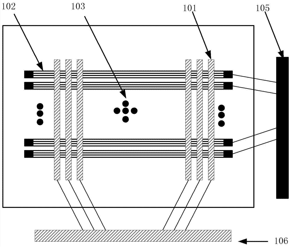
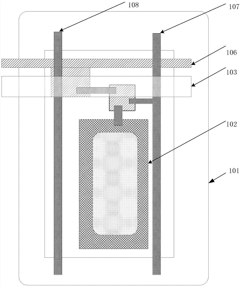
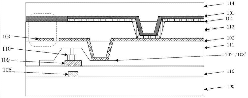
[0023] The basic scheme of the present invention is to use the anode and cathode layers of the OLED device as the electrode layer of the touch sensor, that is, the cathode is patterned and then used as the sensing electrode Rx of the sensing layer of the touch sensor, and is arranged on the substrate in conjunction with the touch sensor. At least one touch drive electrode set on the same layer as the anode is used as the drive electrode Tx of the touch sensor; and then the OLED drive operation and touch sensing operation are performed through time-sharing driving to complete this integrated in-cell touch display touch and display operations. The solution of the embod...


PUM


Abstract

The present invention proposes an OLED touch substrate, comprising: a substrate; an anode and a cathode arranged on the substrate, the anode includes a plurality of sub-anodes, and the cathode includes a plurality of sub-cathodes; the anode is arranged on the same layer as the anode on the substrate At least one touch drive electrode is provided, the touch drive electrode is insulated from the cathode, and is arranged across the sub-cathode; in the display stage, a display drive signal is applied to the cathode and the anode, so The display driving signal is used to drive the OLED light-emitting device; in the touch stage, the touch driving signal is applied to the touch driving electrode, and the sub-anode is used as a touch sensing electrode to output a touch sensing signal. The present invention also proposes a display device including the above-mentioned OLED touch substrate and a driving method thereof. The present invention uses the anode and cathode layers of the OLED device as electrode layers for touch control, realizes touch control and display of the touch display screen through time-sharing driving, saves electrode layers, and can prepare thinner touch display screens.

Description

technical field [0001] The present invention relates to the display field, in particular to a touch substrate, a display device, a manufacturing method and a driving method thereof. Background technique [0002] Active Matrix / Organic Light Emitting Diode AMOLED (Active Matrix / Organic Light Emitting Diode) is an active matrix organic light emitting diode panel. Compared with traditional liquid crystal panels, AMOLED has attracted much attention because of its advantages such as fast response speed, high brightness, low power consumption, good viewing angle, and flexible display. At present, small and medium-sized AMOLED displays mostly adopt on-cell touch (On-cell touch) technology. Compared with the on-unit touch technology, the AMOLED in-cell technology has gradually attracted attention because it can make the display module thinner and lighter. [0003] Most of the AMOLED embedded solutions that have been reported are to make the sensor under the package substrate, but t...

Claims


Application Information

Patent Timeline
Patent Type & Authority Patents(China)
IPC IPC(8): G06F3/041G06F3/044
CPCG02F1/13338G06F3/0412G06F2203/04103G06F3/04166G06F3/0446G06F3/0445H10K59/40H10K50/813H10K50/822H10K59/1216G06F3/041
Inventor 逯家宁石领王龙刘利宾
Owner BOE TECH GRP CO LTD
Why Eureka
Try Eureka