Manufacturing method for circuit board capable of detecting inner-layer pore ring

A manufacturing method and circuit board technology, applied in the direction of multi-layer circuit manufacturing, circuit inspection/monitoring/correction, etc., can solve the problems of circuit board inflow, customer claims, circuit board defects, etc.

Inactive Publication Date: 2015-09-16
SHENZHEN SUNTAK MULTILAYER PCB
View PDF5 Cites 8 Cited by
  • Summary
  • Abstract
  • Description
  • Claims
  • Application Information

AI Technical Summary

Problems solved by technology

[0002] During the production process of the printed circuit board, due to the comprehensive factors of the alignment accuracy of the inner layer graphics, the alignment accuracy of the lamination and pre-stacking, and the expansion and contraction of the sub-board after lamination, it is impossible to guarantee that all PCB boards meet the requirements after drilling the sub-board. IPC3 level standard: that is, the annular ring of the metallized hole of each sub-board in the inner layer is ≥0.025mm
In some circuit board applications, it is required that the annular ring in the inner layer of all circuit boards must be ≥ 0.025mm. If 3-5 boards are taken out and sent to a third-party laboratory for slice detection, and the annular ring does not meet the IPC3 standard, it will be judged as a whole The first batch of circuit boards is defective, so the production of circuit boards that meet the requirements of such standards, if the inner ring is found to be less than 0.025mm when making shipments, will be screened one by one by X-ray detection to pick out those that do not meet the standard requirements Circuit board scrap
However, since X-RAY inspection can only use the naked eye to identify boards with partial holes or serious layers, it is impossible to quantify the size of the inner annular ring of each layer, so it is still possible that the inner annular ring is less than 0.025mm The circuit board flowed into the customer and caused a claim

Method used


Image

  • Manufacturing method for circuit board capable of detecting inner-layer pore ring
  • Manufacturing method for circuit board capable of detecting inner-layer pore ring
  • Manufacturing method for circuit board capable of detecting inner-layer pore ring

Examples


Embodiment

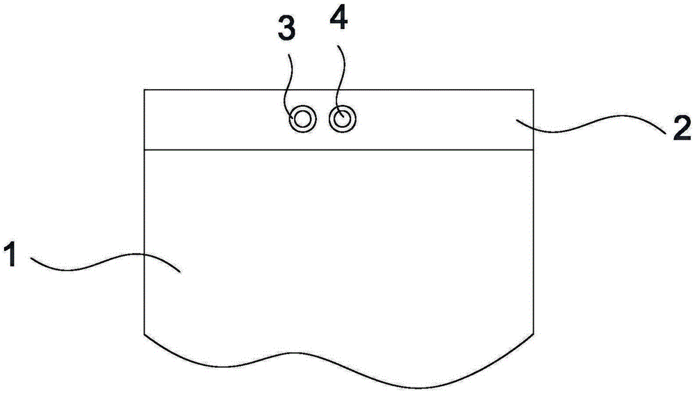
[0020] Such as figure 1 As shown, the circuit board includes a PCB unit 1 and a process side 2, and the inner annular ring in the PCB unit 1 is required to be ≥0.025mm. The minimum annular ring width in PCB unit 1 is 0.125mm, corresponding to the drilling aperture diameter of the smallest annular ring is 0.1mm (that is, the annular ring surrounds the drill hole, and the outer diameter of the annular ring is 0.35mm. Two windows 3 are provided on the process side 2, and the window There is no copper at position 3, the hole diameter of window 3 is 0.3mm, the window position is provided with auxiliary hole 4, and the hole diameter of auxiliary hole 4 is 0.1mm; The layer is not connected to the copper lines in PCB unit 1.

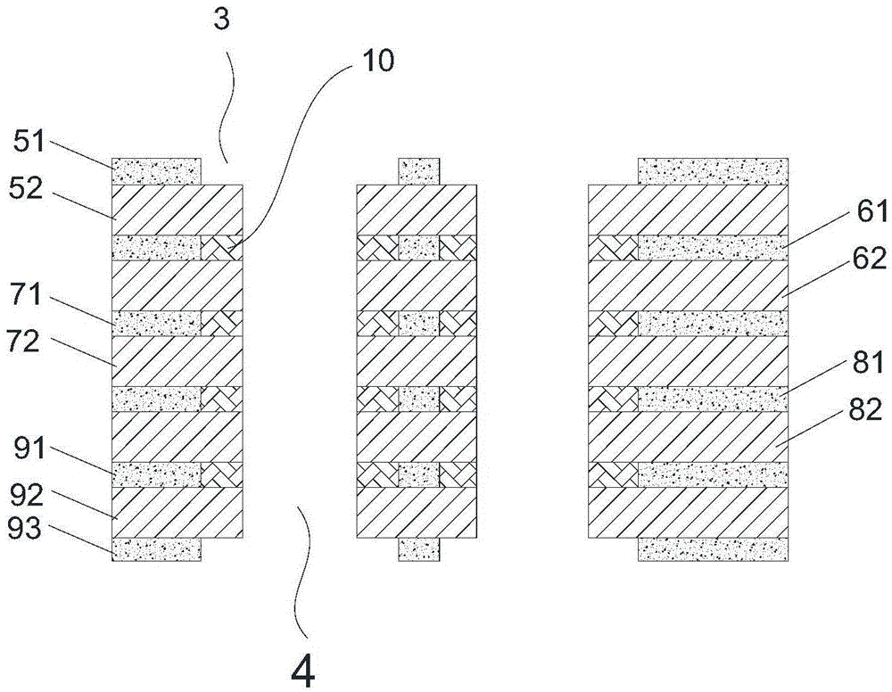
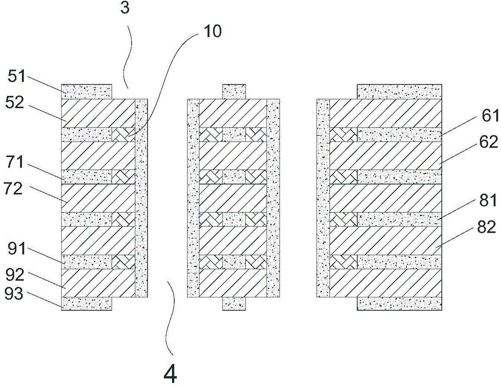
[0021] Such as figure 2 The circuit board is a six-layer circuit board, which is formed by pressing five sub-boards. The first sub-board includes the first copper layer 51 and the first core board 52, and the second sub-board includes the second copper layer ...


PUM


Abstract

The present invention discloses a manufacturing method for a circuit board capable of detecting an inner-layer hole ring and relates to the technical field of production of circuit boards. The manufacturing method comprises: providing a secondary board for pressing and manufacturing the circuit board, wherein the secondary board comprises a PCB unit and a technical edge; manufacturing a circuit pattern in the PCB unit of each secondary board; meanwhile, etching at least two windows at a corresponding position on the technical edge of each secondary board, wherein the diameter of each window is 0.05mm smaller than the outer diameter of a smallest hole ring designed in the PCB unit; pressing each secondary board into the circuit board; drilling a borehole in the PCB unit and drilling an auxiliary hole at the central position of the window on the surface of the technical edge; manufacturing the borehole and the auxiliary hole in the PCB unit into metallized holes; and manufacturing a short-circuit test point of the auxiliary hole. The detection method provided by the present invention can ensure that the inner-layer hole ring of the manufactured circuit board has the diameter that is more than or equal to 0.025mm and meets IPC3 stage standard, is applicable to the circuit board that is particularly indicated that the diameter of the hole ring is required to be controlled to be more than or equal to 0.025mm, so as to effectively avoid complaints resulting from the defect of the inner-layer hole ring and the risk of the whole batch being returned and scrapped due to failure in a sample test.

Description

technical field [0001] The invention belongs to the technical field of circuit board production, in particular to a circuit board manufacturing method capable of detecting inner-layer annular rings. Background technique [0002] During the production process of the printed circuit board, due to the comprehensive factors of the alignment accuracy of the inner layer graphics, the alignment accuracy of the lamination and pre-stacking, and the expansion and contraction of the sub-board after lamination, it is impossible to guarantee that all PCB boards meet the requirements after drilling the sub-board. IPC3 level standard: that is, the hole ring of the metallized hole of each sub-board of the inner layer is ≥0.025mm. In some circuit board applications, it is required that the annular ring in the inner layer of all circuit boards must be ≥ 0.025mm. If 3-5 boards are taken out and sent to a third-party laboratory for slice detection, and the annular ring does not meet the IPC3 st...

Claims


Application Information

Patent Timeline
Patent Type & Authority Applications(China)
IPC IPC(8): H05K3/46
CPCH05K3/46H05K2203/16
Inventor 刘林武樊锡超季辉喻恩
Owner SHENZHEN SUNTAK MULTILAYER PCB
Why Eureka
Try Eureka