

DICE structure latch unit resisting single-particle irradiation effect
An anti-single-event radiation, latching unit technology, applied in electrical components, logic circuits, pulse technology, etc., can solve problems such as large dynamic power consumption, reduce dynamic power consumption, and reduce the possibility of simultaneous conduction Effect
Inactive Publication Date: 2015-11-11
NORTHWESTERN POLYTECHNICAL UNIV
View PDF6 Cites 15 Cited by
- Summary
- Abstract
- Description
- Claims
- Application Information
AI Technical Summary
Problems solved by technology
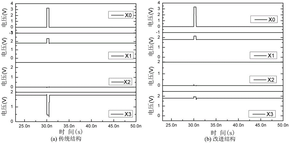
[0006] In order to overcome the deficiency of large dynamic power consumption of the existing DICE structure la
Method used
View moreImage
Smart ImageViewing Examples

Examples
 PUM
 Abstract
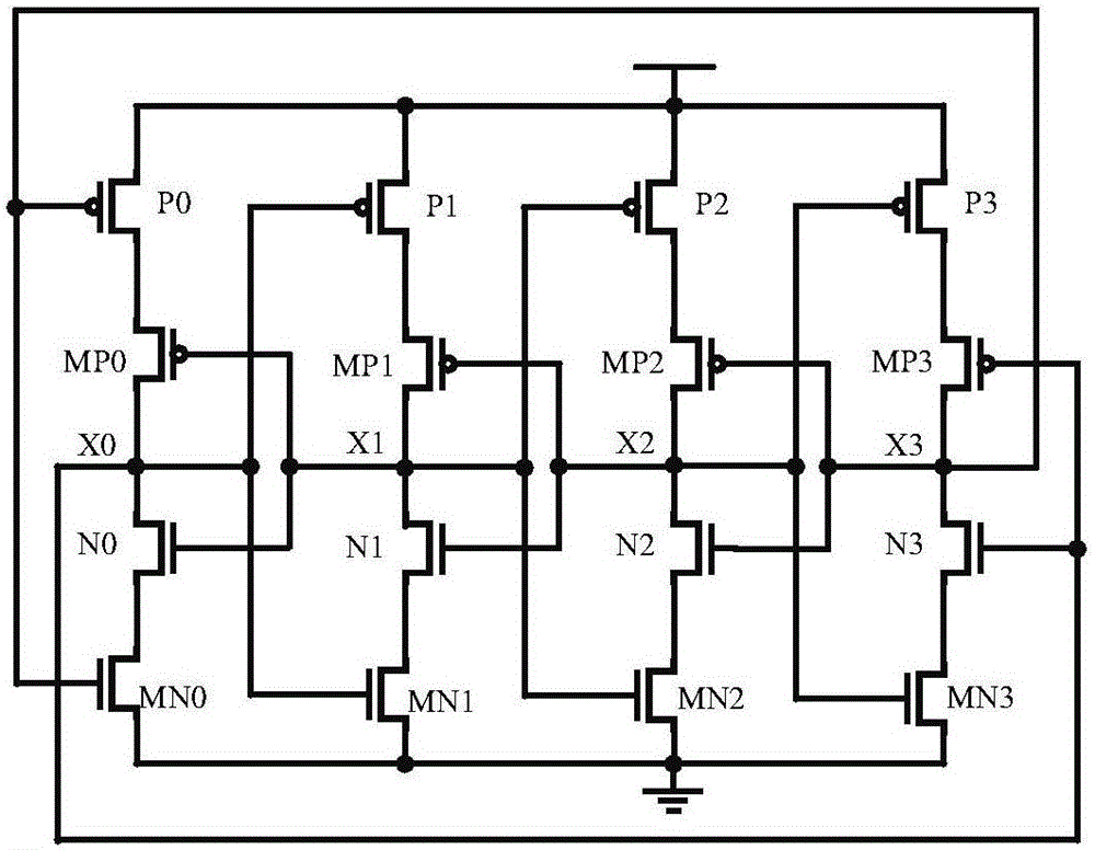
The invention discloses a DICE structure latch unit resisting single-particle irradiation effect, which is used for solving the technical problem of large dynamic power consumption of the conventional DICE structure latch unit. The DICE structure latch unit comprises a P-channel metal oxide semiconductor (PMOS) transistor P0, a PMOS transistor P1, a PMOS transistor P2, a PMOS transistor P3, an N-channel metal oxide semiconductor (NMOS) transistor N0, an NMOS transistor N1, an NMOS transistor N2, and an NMOS transistor N3, and also comprises an NMOS transistor MN0, an NMOS transistor MN1, an NMOS transistor MN2, an NMOS transistor MN3, a PMOS transistor MP0, a PMOS transistor MP1, a PMOS transistor MP2, and a PMOS transistor MP3. The NMOS transistor MN0, the NMOS transistor MN1, the NMOS transistor MN2 and the NMOS transistor MN3 and the PMOS transistor P0, the PMOS transistor P1, the PMOS transistor P2 and the PMOS transistor P3 are complementary. The PMOS transistor MP0, the PMOS transistor MP1, the PMOS transistor MP2 and the PMOS transistor MP3 and the NMOS transistor N0, the NMOS transistor N1, the NMOS transistor N2 and the NMOS transistor N3 are complementary. Due to adoption of the method of MOS transistor insertion complementation, direct impact between adjacent nodes is prevented, and the probability that the PMOS transistors and NMOS transistors of each branch are conducted simultaneously is lowered. The expected effect that overturn of any one of four storage nodes does not cause overturn of the other three is achieved, so that the dynamic power consumption of the DICE structure latch unit is reduced.
Description
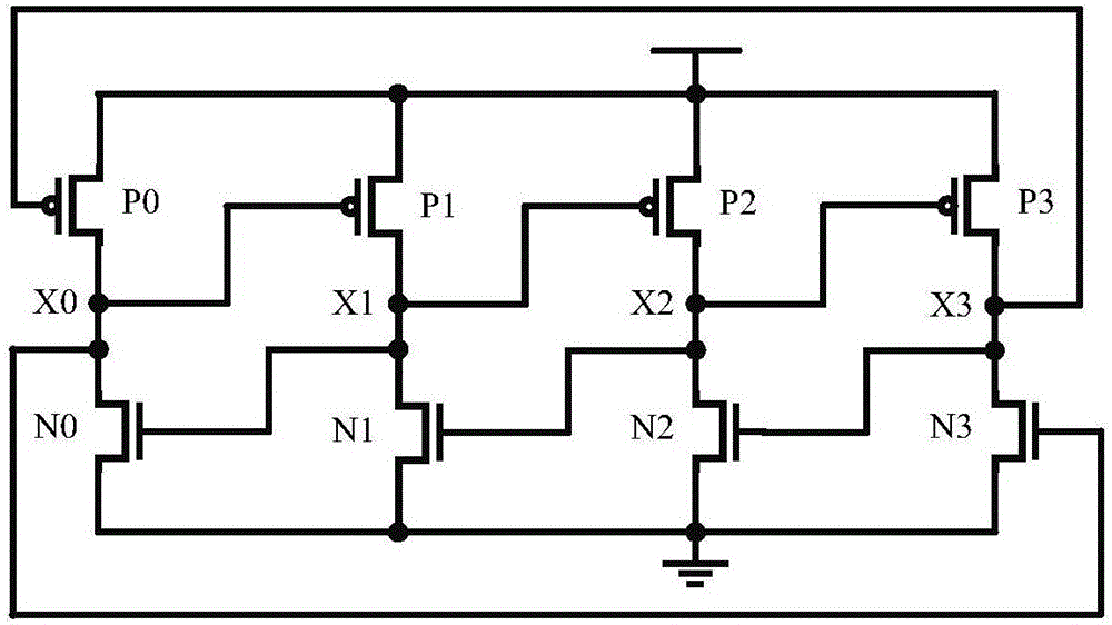
technical field [0001] The invention relates to a DICE structure latch unit, in particular to a DICE structure latch unit which can resist single event radiation effect. Background technique [0002] refer to figure 1 . The document "T. Calin, M. Nicolaidis, and R. Velazco, "Upset Hardened Memory Design for Submicron CMOS Technology," IEEE Trans. Nuclear Science, vol. 43, no. 6, pp. 2874-2878, Dec. 1996" discloses a DICE structure latch unit. The latch structure is composed of four PMOS transistors P0 to P3 and four NMOS transistors N0 to N3. This structure has four storage nodes X0, X1, X2, X3. When the X0 node to the X3 node are 0101 respectively, if a 0-1 flip occurs at the X0 node, this flip will turn on the NMOS transistor N3, so a 1-0 flip occurs at the X3 node, but this flip will not affect the X1 node and X2 node. Similarly, if a 1-0 inversion occurs at the X1 node, this inversion will turn on the PMOS transistor P2, so that a 0-1 inversion occurs at the X2 node...
Claims
Login to View More Application Information
Patent Timeline
 IPC IPC(8): H03K19/0944
Inventor高武刘辉王佳魏晓敏胡永才
OwnerNORTHWESTERN POLYTECHNICAL UNIV