A high-precision probe loading device for pcb automatic test equipment

A technology of automatic test equipment and loading device, which is used in measurement devices, electronic circuit testing, printed circuit testing, etc., can solve the problems of small probe pressure adjustment range, complex mechanical structure, low loading accuracy, etc., and achieve reasonable and reliable structural design. , to prevent probe damage, the effect of convenient processing

Active Publication Date: 2018-08-07
ZHONGBEI UNIV
View PDF6 Cites 0 Cited by
  • Summary
  • Abstract
  • Description
  • Claims
  • Application Information

AI Technical Summary

Problems solved by technology

[0004] The present invention provides a high-precision probe loading device for PCB automatic testing equipment in order to solve the problems of complex mechanical structure, small adjustment range of probe stroke and probe pressure and low loading accuracy existing in the existing probe loading device.

Method used


Image

  • A high-precision probe loading device for pcb automatic test equipment
  • A high-precision probe loading device for pcb automatic test equipment

Examples


Embodiment Construction

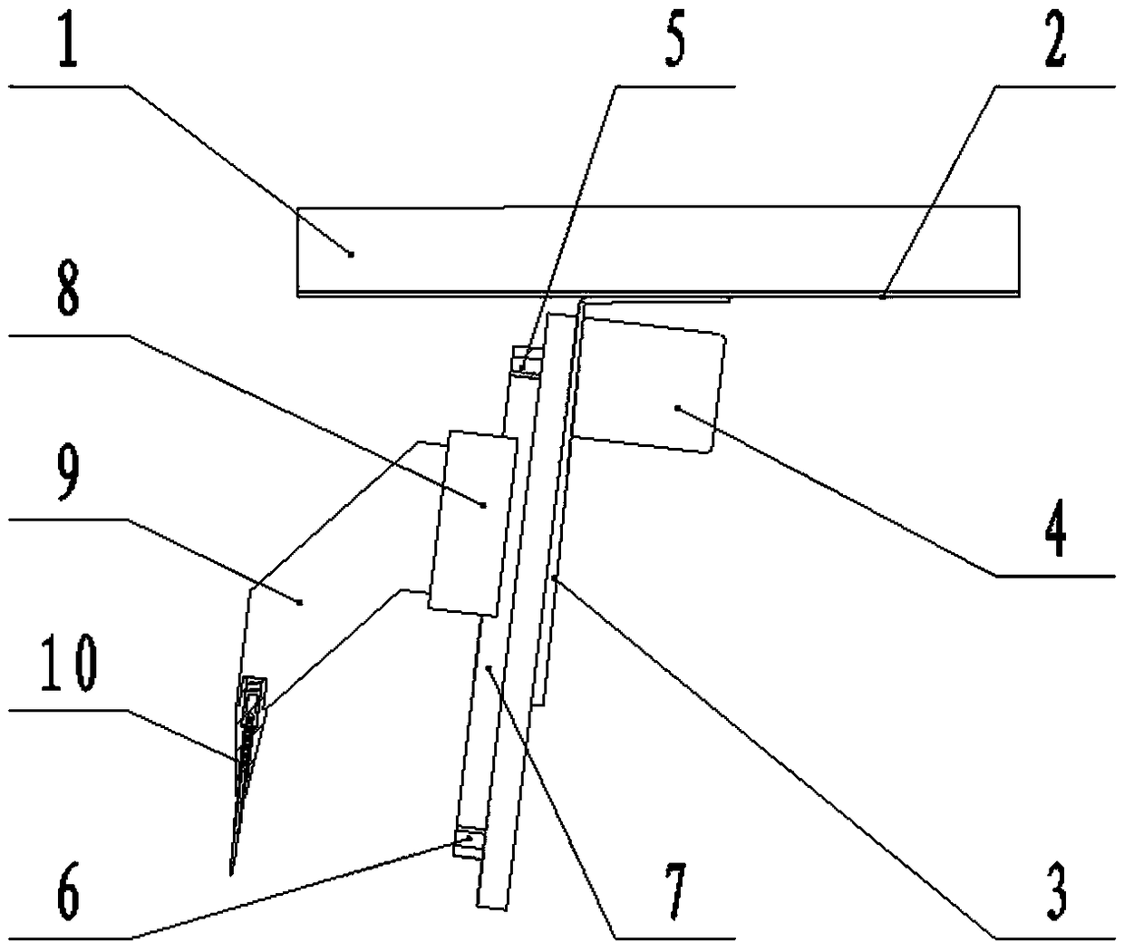
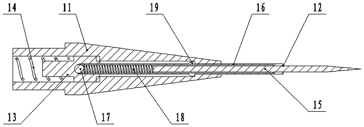
[0011] A high-precision probe loading device for PCB automatic test equipment, including a mover body 1 that moves along the X / Y direction of the test equipment. The support 3, the linear motor 4 is fixed on one side of the support 3, the other side of the support 3 is provided with a driving wheel 5 and a driven wheel 6, the driving wheel 5 is connected with the output shaft of the linear motor 4, and the driving wheel 5 and the driven wheel 6 is provided with a transmission belt 7, the transmission belt 7 is provided with a slider 8, the slider 8 is provided with an insulating block 9, the lower end of the insulating block 9 is provided with a probe assembly 10, and the probe assembly 10 includes a The sleeve 11 in 9 has a probe 12 inside the sleeve 11. The tail of the probe 12 has a stepped positioning block 13 that is in contact with the inner wall of the sleeve 11. The tail of the stepped positioning block 13 is covered with a contact with the insulating block 9. The buff...


PUM


Abstract

The invention specifically provides a high-precision probe loading device used for a PCB automatic testing device and solves the problems that an existing probe loading device is complex in mechanical structure, small in probe stroke and probe pressure adjusting range and low in loading precision. A support is arranged on the surface of a mover body. A linear motor is fixed at one side of the support. The other side of the support is provided with a driving wheel and a driven wheel. A transmission belt is arranged between the driving wheel and the driven wheel. A sliding block is arranged on the transmission belt. The sliding block is provided with an insulating block. The lower end of the insulating block is provided with a probe assembly. The probe assembly comprises a sleeve. A probe is arranged in the sleeve in a penetrating manner. The tail part of the probe is abutted against a stepped positioning block. The tail part of the stepped positioning block is sleeved by a buffering spring. The probe is composed of a probe body and a probe sleeve, and the probe sleeve is internally provided with a steel ball. A probe buffering spring is arranged between the steel ball and the tail part of the probe body. The probe body and the side wall of the probe are respectively provided with an anti-falling boss. By adopting the high-precision probe loading device, a loading precision index of a tested point is ensured.

Description

technical field [0001] The invention relates to a probe loading device, in particular to a high-precision probe loading device for PCB automatic testing equipment. Background technique [0002] In the circuit board automatic test system, the instrument realizes the test by contacting the test point on the circuit board under test with the probe controlled by the computer to extract the signal; the usual circuit board automatic test equipment (such as flying probe tester, etc.) consists of more than one Probe component composition; when the test equipment is working, the action of probe loading can be decomposed into the action of the probe displacement positioning (usually referring to the X / Y direction) mechanism and the probe assembly controlling the loading of the probe in the vertical direction (usually referring to the Z direction) Actions. [0003] The existing probe loading device has problems such as complex mechanism, small probe height and loading pressure range, ...

Claims


Application Information

Patent Timeline
Patent Type & Authority Patents(China)
IPC IPC(8): G01R1/073G01R31/28
CPCG01R1/07392G01R31/2801
Inventor 刘新妹殷俊龄富强郭鑫
Owner ZHONGBEI UNIV
Why Eureka
Try Eureka