Eureka AIR delivers breakthrough ideas for toughest innovation challenges, trusted by R&D personnel around the world.

A method of manufacturing a pcb

A production method and technology of resisting glue, applied in multilayer circuit manufacturing, printed circuit manufacturing, printed circuit and other directions, can solve the problems of semi-cured P-chip not belonging to high-frequency and high-speed materials, restricting use, signal loss, etc., to improve the signal Transmission quality and speed, the effect of expanding the application

Active Publication Date: 2019-01-25
DONGGUAN SHENGYI ELECTRONICS
View PDF8 Cites 0 Cited by
  • Summary
  • Abstract
  • Description
  • Claims
  • Application Information

AI Technical Summary

Problems solved by technology

[0003] It is difficult to embed the closed cavity inside the PCB. At present, in order to control the glue flow inside the closed cavity and the shape of the cavity, most designs use pre-cured P sheets that do not flow or have low fluidity for lamination, but this type of semi-cured Cured P-chip is not a high-frequency and high-speed material, and has a certain loss on the signal. At the same time, the above design restricts the use of high-frequency, high-speed and conventional P-chip materials in PCBs.

Method used


Image

  • A method of manufacturing a pcb
  • A method of manufacturing a pcb
  • A method of manufacturing a pcb

Examples


Embodiment 1

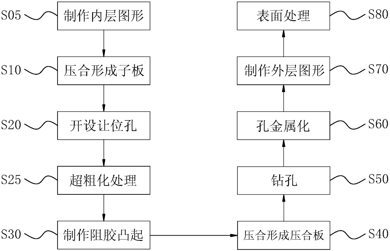
[0050] like figure 1 and figure 2 Shown, a kind of manufacturing method of PCB comprises the following steps:

[0051] S05, making the inner layer graphics on the inner layer core board;

[0052] S10. Provide the inner core board 21 and the prepreg 5 that need to be perforated, and press the inner core board 21 and the prepreg 5 that need to be perforated to form a sub-board 2;

[0053] S20. Opening a relief hole 22 on the sub-board 2;

[0054] S25. Perform super-roughening treatment on the sub-board 2;

[0055] S30, making glue-resisting protrusions 4 on the end surface of the sub-board 2 and at the edge of the relief hole 22;

[0056] S40, providing a non-perforated core board and a prepreg 5, and pressing the non-perforated core board, the prepreg 5 and the sub-board 2 to form a laminated board with a closed cavity;

[0057] S50, drilling the laminated board, and performing post-drilling treatment;

[0058] S60, performing electroless copper deposition and electropla...

Embodiment 2

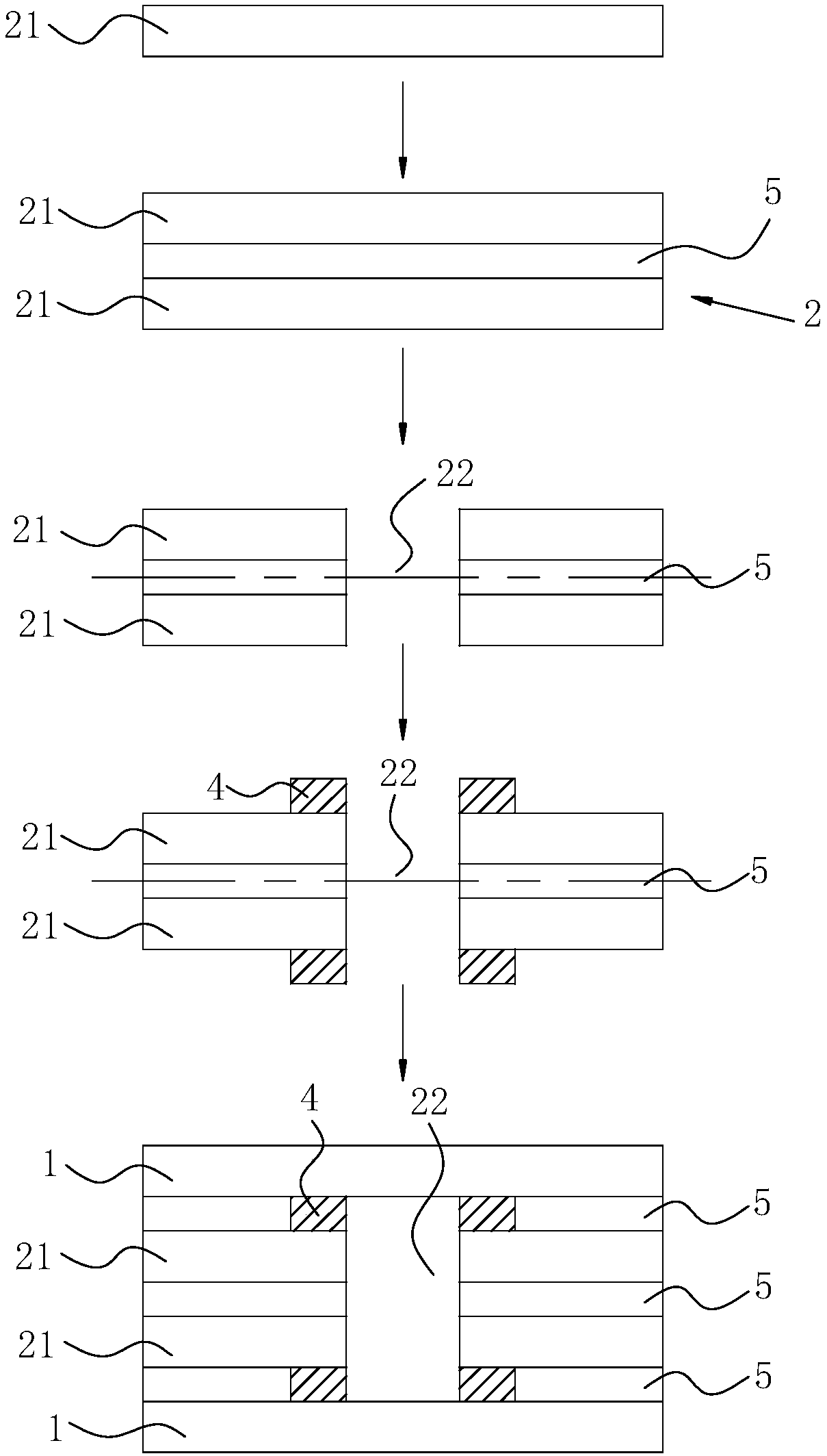
[0072] like figure 1 and image 3 Shown, a kind of manufacturing method of PCB comprises the following steps:

[0073] S05. Making an inner layer pattern on the inner layer core board.

[0074] S10. Provide the inner core board 21 and the prepreg 5 that need to be perforated, and press the inner core board 21 and the prepreg 5 that need to be perforated to form a sub-board 2;

[0075] S20. Opening a relief hole 22 on the sub-board 2;

[0076] S25 , performing super-roughening treatment on the sub-board 2 .

[0077] S30, making glue-resisting protrusions 4 on the end surface of the sub-board 2 and at the edge of the relief hole 22;

[0078] S40 , providing a non-perforated core board and a prepreg 5 , and pressing the non-perforated core board, the prepreg 5 and the sub-board 2 to form a laminated board with a closed cavity.

[0079] S50, drilling the laminated board, and performing post-drilling treatment;

[0080] S60, performing electroless copper deposition and electr...

Embodiment 3

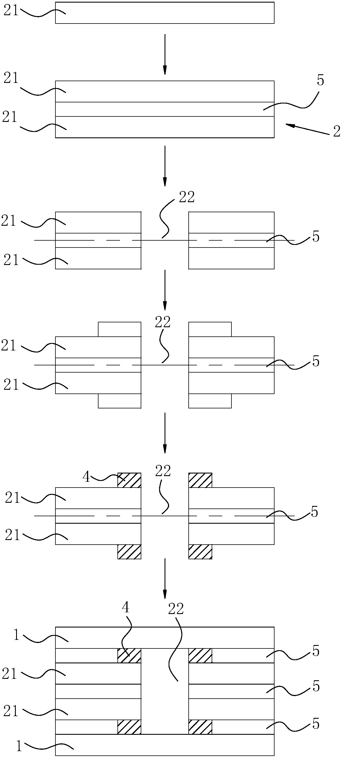
[0096] like figure 1 and Figure 4 Shown, a kind of manufacturing method of PCB comprises the following steps:

[0097] S05. Making an inner layer pattern on the inner layer core board.

[0098] S10. Provide the inner core board 21 and the prepreg 5 that need to be perforated, and press the inner core board 21 and the prepreg 5 that need to be perforated to form a sub-board 2;

[0099] S20. Opening a relief hole 22 on the sub-board 2;

[0100] S25 , performing super-roughening treatment on the sub-board 2 .

[0101] S30, making glue-resisting protrusions 4 on the end surface of the sub-board 2 and at the edge of the relief hole 22;

[0102] S40 , providing a non-perforated core board and a prepreg 5 , and pressing the non-perforated core board, the prepreg 5 and the sub-board 2 to form a laminated board with a closed cavity.

[0103] S50, drilling the laminated board, and performing post-drilling treatment;

[0104] S60, performing electroless copper deposition and elect...


PUM


Abstract

The invention discloses a manufacturing method of a PCB. The manufacturing method comprises the following steps: S10, providing a pored inner layer core plate and a prepreg, and laminating the pored inner layer core plate and the prepreg to form a sub-plate; S20, forming an avoidance hole in the sub-plate; S30, manufacturing a rubber blocking bulge on the end surface of the sub-plate and at the position of the edge of the avoidance hole; and S40, providing a non-pored core plate and a prepreg, and laminating the non-pored core plate, the prepreg and the sub-plate to form a laminating plate with a sealing cavity. In the scheme, through twice laminating forming, firstly the pored inner layer core plate is laminated to form the sub-plate, and the avoidance hole is integrally formed in the sub-plate, so that the smoothness of inner wall shape of the avoidance hole is guaranteed; and then the rubber blocking bulge is arranged at the edge of the avoidance hole, and the sub-plate and the non-pored core plate are laminated to form the laminating plate, so that internal gumming of the sealing cavity can be effectively controlled, the integrality of the inner wall shape is guaranteed; and meanwhile, the application of high-frequency and high-speed materials in the PCB is widened, and the quality and speed of signal transmission are promoted.

Description

technical field [0001] The invention relates to the technical field of PCB production, in particular to a method for manufacturing a PCB. Background technique [0002] Electronic products are indispensable tools for modern life and work. People have higher and higher requirements for the performance of electronic products, and the acceleration of signal transmission speed and the reduction of process loss are the main requirements of electronic products at present. At present, the methods to increase signal propagation speed and reduce loss mainly include reducing the dielectric constant of materials, improving stacking, and circuit design. In order to meet the high requirements of electronic products for signal quality, the high-end design of embedding a closed cavity inside the PCB can not only increase the signal transmission speed of the circuit board, but also further reduce the signal loss. [0003] It is difficult to embed the closed cavity inside the PCB. At present...

Claims


Application Information

Patent Timeline
Patent Type & Authority Patents(China)
IPC IPC(8): H05K3/46
CPCH05K3/4697H05K2203/052
Inventor 傅宝林纪成光李民善袁继旺
Owner DONGGUAN SHENGYI ELECTRONICS
Why Eureka
Eureka Blog
Learn More