

Manufacturing method of PCB
A production method and glue-resistance technology, which is applied in multilayer circuit manufacturing, printed circuit manufacturing, electrical components, etc., can solve the problems of semi-cured P sheet not belonging to high-frequency and high-speed materials, restricting use, and signal loss, etc., to improve signal Transmission quality and speed, and the effects of expanded use
- Summary
- Abstract
- Description
- Claims
- Application Information
AI Technical Summary
Problems solved by technology
Method used
Image

Examples
Embodiment 1
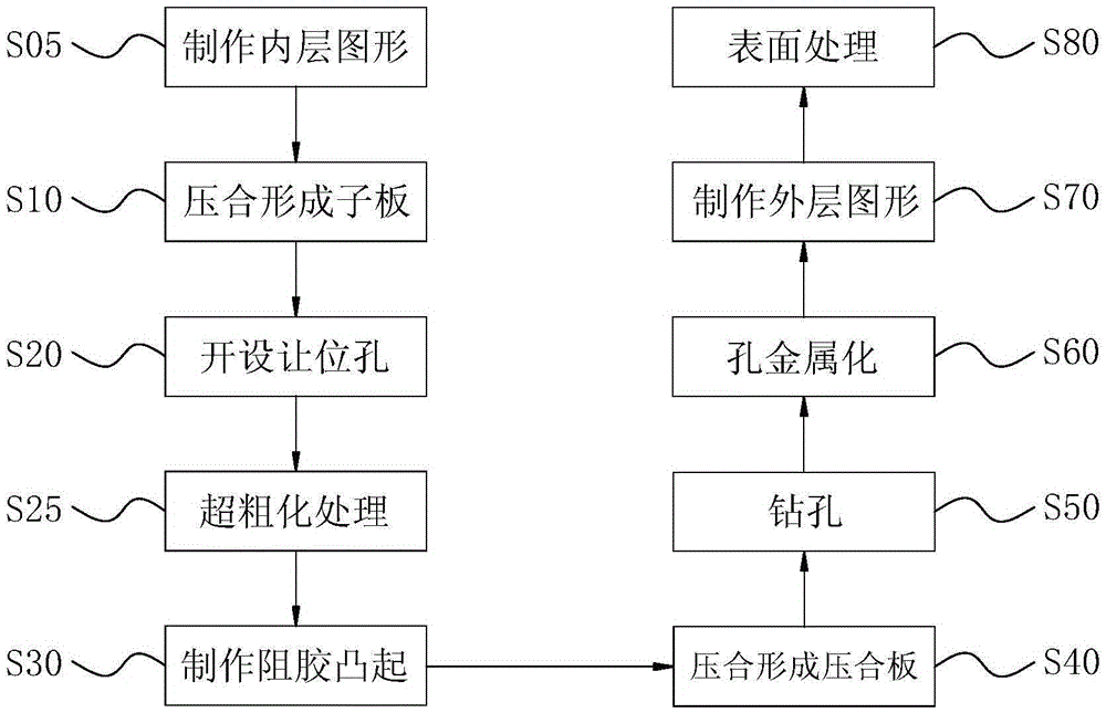
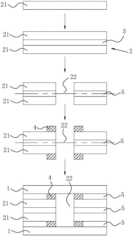
[0050] Such as figure 1 with figure 2 Shown, a kind of manufacturing method of PCB comprises the following steps:
[0051] S05, making the inner layer graphics on the inner layer core board;
[0052] S10. Provide the inner core board 21 and the prepreg 5 that need to be perforated, and press the inner core board 21 and the prepreg 5 that need to be perforated to form a sub-board 2;
[0053] S20. Opening a relief hole 22 on the sub-board 2;
[0054] S25. Perform super-roughening treatment on the sub-board 2;
[0055] S30, making glue-resisting protrusions 4 on the end surface of the sub-board 2 and at the edge of the relief hole 22;
[0056] S40, providing a non-perforated core board and a prepreg 5, and pressing the non-perforated core board, the prepreg 5 and the sub-board 2 to form a laminated board with a closed cavity;
[0057] S50, drilling the laminated board, and performing post-drilling treatment;
[0058] S60, performing electroless copper deposition and electr...
Embodiment 2
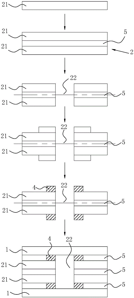
[0072] Such as figure 1 with image 3 Shown, a kind of manufacturing method of PCB comprises the following steps:
[0073] S05. Making an inner layer pattern on the inner layer core board.
[0074] S10. Provide the inner core board 21 and the prepreg 5 that need to be perforated, and press the inner core board 21 and the prepreg 5 that need to be perforated to form a sub-board 2;
[0075] S20. Opening a relief hole 22 on the sub-board 2;
[0076] S25 , performing super-roughening treatment on the sub-board 2 .
[0077] S30, making glue-resisting protrusions 4 on the end surface of the sub-board 2 and at the edge of the relief hole 22;
[0078] S40 , providing a non-perforated core board and a prepreg 5 , and pressing the non-perforated core board, the prepreg 5 and the sub-board 2 to form a laminated board with a closed cavity.
[0079] S50, drilling the laminated board, and performing post-drilling treatment;
[0080] S60, performing electroless copper deposition and el...
Embodiment 3
[0096] Such as figure 1 with Figure 4 Shown, a kind of manufacturing method of PCB comprises the following steps:
[0097] S05. Making an inner layer pattern on the inner layer core board.
[0098] S10. Provide the inner core board 21 and the prepreg 5 that need to be perforated, and press the inner core board 21 and the prepreg 5 that need to be perforated to form a sub-board 2;
[0099] S20. Opening a relief hole 22 on the sub-board 2;
[0100] S25 , performing super-roughening treatment on the sub-board 2 .
[0101] S30, making glue-resisting protrusions 4 on the end surface of the sub-board 2 and at the edge of the relief hole 22;
[0102] S40 , providing a non-perforated core board and a prepreg 5 , and pressing the non-perforated core board, the prepreg 5 and the sub-board 2 to form a laminated board with a closed cavity.
[0103] S50, drilling the laminated board, and performing post-drilling treatment;
[0104] S60, performing electroless copper deposition and e...
PUM
 Abstract
Description
Claims
Application Information