A kind of temperable triple-silver low-emissivity coated glass and preparation method thereof
A low-emissivity coating and magnetron sputtering coating technology, applied in the field of glass, can solve the problems of unstable color, color channel, complex film structure, etc., and achieve the effect of improving scratch resistance and color stability
- Summary
- Abstract
- Description
- Claims
- Application Information
AI Technical Summary
Problems solved by technology
Method used
Image
Examples
Embodiment 1
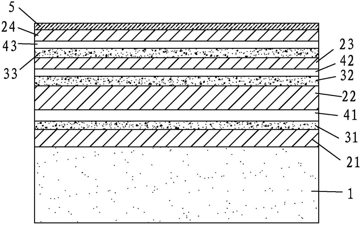
[0024] See figure 1 , a temperable triple-silver low-emissivity coated glass, the structure is: glass substrate 1 / first composite dielectric layer 21 [silicon nitride (thickness 10nm), zinc oxide (5nm), AZO (10nm)] / first Silver layer 31 (15nm) / nickel-chromium 41 (1nm) / second composite dielectric layer 22 [silicon nitride (20nm), zinc tin oxide (40nm), zinc oxide (10nm), AZO (5nm)] second silver layer 32 (15nm) / nickel-chromium 42 (1nm) / third composite dielectric layer 23 [silicon nitride (20nm), zinc tin oxide (20nm), zinc oxide (10nm), AZO (10nm)] / third silver layer 33 (5nm) / nickel-chromium 43 (10nm) / fourth composite dielectric layer 24 [AZO (5nm), zinc oxide (20nm), silicon nitride (20nm)] / ZrOx5 (10nm).
Embodiment 2
[0026] A temperable triple-silver low-emissivity coated glass, the structure is: glass substrate / first composite dielectric layer [silicon nitride (thickness 25nm), zinc oxide (15nm), AZO (5nm)] / first silver layer ( 5nm) / nickel-chromium (10nm) / second composite dielectric layer [silicon nitride (40nm), zinc tin oxide (20nm), zinc oxide (20nm), AZO (10nm)] second silver layer (5nm) / nickel-chromium (10nm) / third composite dielectric layer [silicon nitride (40nm), zinc tin oxide (40nm), zinc oxide (20nm), AZO (5nm)] / third silver layer (15nm) / nickel-chromium (1nm) / The fourth composite dielectric layer [AZO (10nm), zinc oxide (10nm), silicon nitride (40nm)] / ZrOx (3nm).
Embodiment 3
[0028] A temperable triple-silver low-emissivity coated glass, the structure is: glass substrate / first composite dielectric layer [silicon nitride (thickness 15nm), zinc oxide (8nm), AZO (8nm)] / first silver layer ( 8nm) / nickel-chromium (3nm) / second composite dielectric layer [silicon nitride (25nm), zinc tin oxide (30nm), zinc oxide (15nm), AZO (6nm)] second silver layer (10nm) / nickel-chromium (3nm) / third composite dielectric layer [silicon nitride (35nm), zinc tin oxide (30nm), zinc oxide (15nm), AZO (6nm)] / third silver layer (10nm) / nickel-chromium (3nm) / The fourth composite dielectric layer [AZO (6nm), zinc oxide (15nm), silicon nitride (25nm)] / ZrOx (5nm).
PUM
| Property | Measurement | Unit |
|---|---|---|
| thickness | aaaaa | aaaaa |
| thickness | aaaaa | aaaaa |
| thickness | aaaaa | aaaaa |
Abstract
Description
Claims
Application Information


