Touch control display device, touch control display panel and array substrate
A touch display panel and array substrate technology, which is applied in the fields of instruments, computing, electrical and digital data processing, etc., can solve the problem of uneven display of the display screen, improve the uneven display, reduce the difference in the number of vias, and improve the vias. uneven effect
- Summary
- Abstract
- Description
- Claims
- Application Information
AI Technical Summary
Problems solved by technology
Method used
Image

Examples
no. 1 example
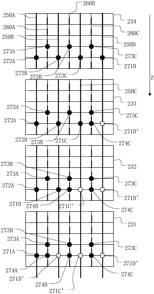
[0053] exist Figure 5 Only a partial view of the array substrate 500 is shown. Figure 5 Touch electrodes 530A and 530B are shown. Figure 5 Eight touch leads 550 are also shown, and each touch lead 550 corresponds to one touch electrode 530 . In other words, a column of touch electrodes with touch electrodes 530A and 530B in the array substrate 500 includes eight touch electrodes 530, and the touch electrodes 530A and 530B are the fourth and fifth touch electrodes in the eight touch electrodes 530. control electrode. Although in Figure 5 Each touch wire 550 corresponds to one touch electrode 530 , but in practical applications, an embodiment in which multiple touch wires 550 correspond to one touch electrode 530 is also possible. exist Figure 5 Among them, the touch lead 550A is connected to the touch electrode 530A through the first via hole 571A, and the touch lead 550B is connected to the touch electrode 530B through the first via hole 571B, and connected to the to...
no. 2 example
[0062] exist Image 6 Only a partial view of the array substrate 600 is shown. Image 6 Touch electrode 630A and touch electrode 630B are shown. Image 6 Eight touch leads 650 are also shown, and every two touch leads 650 correspond to one touch electrode 630 . In other words, a column of touch electrodes with touch electrodes 630A and 630B in the array substrate 600 includes four touch electrodes 630, and the touch electrodes 630A and 630B are the second and third touch electrodes of the four touch electrodes 630. control electrode. exist Image 6 Among them, the two touch leads 650A are connected to the touch electrodes 630A through the first via holes 671A, the two touch leads 650B are connected to the touch electrodes 630B through the first via holes 671B, and connected to the touch electrodes 630B through the second via holes 672B. The touch electrode 630A is connected.
[0063] The two touch leads 650 on the left side of the touch lead 650A are in Image 6 In this ...
no. 3 example
[0068] exist Figure 7 Only a partial view of the array substrate 700 is shown. Figure 7 Touch electrode 730A and touch electrode 730B are shown. Figure 7 Eight touch leads 750 are also shown, and each touch lead 750 corresponds to one touch electrode 730 . In other words, a row of touch electrodes with touch electrodes 730A and 730B in the array substrate 700 includes eight touch electrodes 730, and the touch electrodes 730A and 730B are the fourth and fifth touch electrodes among the eight touch electrodes 730. control electrode. exist Figure 7 Among them, the touch lead 750A is connected to the touch electrode 730A through the first via hole 771A, and the touch lead 750B is connected to the touch electrode 730B through the first via hole 771B, and connected to the touch electrode 730A through the second via hole 772B. connect.
[0069] The three touch leads 750 to the left of touch leads 750A are in Figure 7 In this example, a touch electrode 730 above the touch e...
PUM
 Abstract
Description
Claims
Application Information
 - R&D
- Intellectual Property
- Life Sciences
- Materials
- Tech Scout
- Unparalleled Data Quality
- Higher Quality Content
- 60% Fewer Hallucinations
Browse by: Latest US Patents, China's latest patents, Technical Efficacy Thesaurus, Application Domain, Technology Topic, Popular Technical Reports.
© 2025 PatSnap. All rights reserved.Legal|Privacy policy|Modern Slavery Act Transparency Statement|Sitemap|About US| Contact US: help@patsnap.com