This helps you quickly interpret patents by identifying the three key elements:
Problems solved by technology
Method used
Benefits of technology
Problems solved by technology
[0012] Therefore, the present invention provides a liquid crystal display element using an oxide semiconductor, which can prevent the decrease of the voltage holding ratio (VHR) of the liquid crystal layer and the increase of the ion density (ID), and solve the problem of white spots, uneven orientation, image sticking, etc. Liquid crystal display elements that display poor problems
Method used
Image
Click on the blue label to locate the original text in one second.
Reading with bidirectional positioning of images and text.
Examples
no. 1 approach >
[0038] A first preferred embodiment of the liquid crystal display element according to the present invention has a thin film transistor using an oxide semiconductor and a specific liquid crystal composition, and generates an electric field in a substantially vertical direction between the first substrate and the second substrate of the liquid crystal display element. Liquid crystal display element. The first preferred embodiment is a liquid crystal display element having electrodes on a first substrate and a second substrate, for example, a transmissive liquid crystal display element using a TN (Twisted Nematic: twisted nematic) type.
[0039] The first preferred embodiment of the liquid crystal display element according to the present invention preferably has a first substrate and a second substrate arranged to face each other, and a liquid crystal layer containing a liquid crystal composition is sandwiched between the first substrate and the second substrate, It also has a p...
no. 2 approach >
[0244] The second embodiment of the liquid crystal display element according to the present invention is a liquid crystal display element having a thin film transistor using an oxide semiconductor and a specific liquid crystal composition, and generating an electric field having a component parallel to the substrate surface of the liquid crystal display element. . The second preferred embodiment is an IPS type liquid crystal display element (InPlane Switching mode Liquid Crystal Display) or an FFS type liquid crystal display element (Fringe Field Switching mode Liquid Crystal Display) which is a kind of IPS type liquid crystal display element.
[0245] An IPS type liquid crystal display element which is a second preferred embodiment of the liquid crystal display element according to the present invention has a first substrate and a second substrate arranged to face each other, and a substrate containing a liquid crystal is sandwiched between the first substrate and the second s...
no. 3 approach >
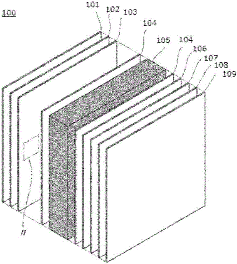
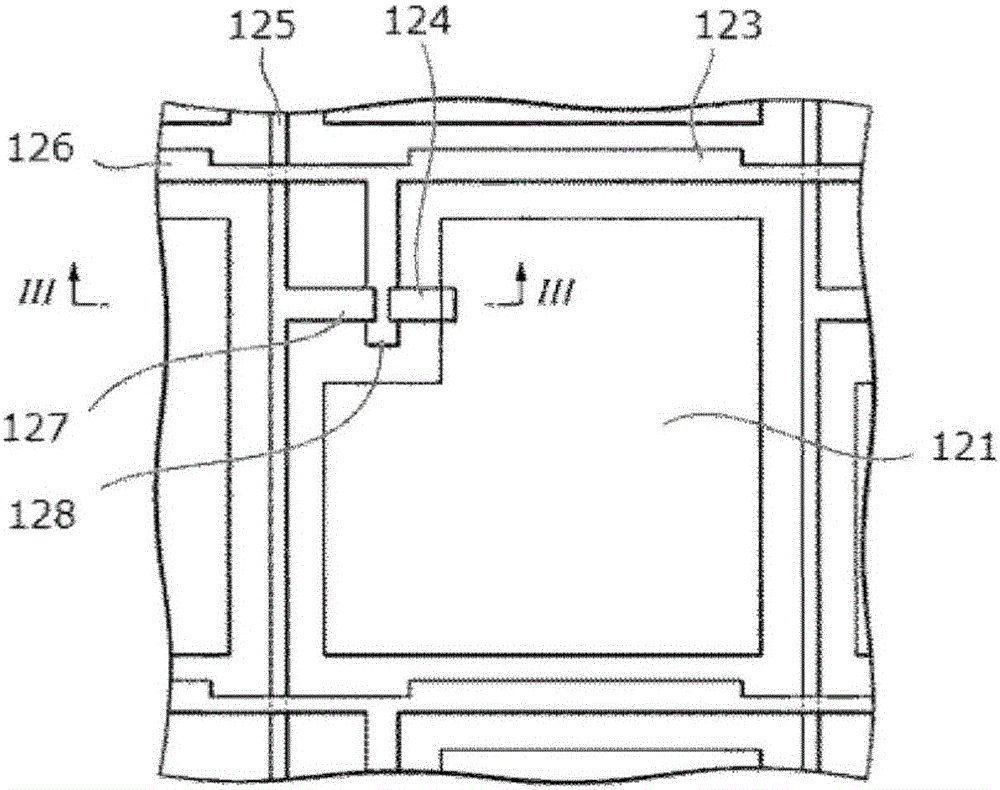
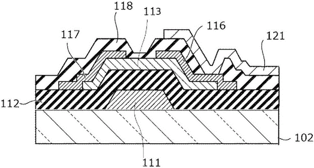
[0268] The configuration of the third embodiment according to the present invention is a liquid crystal display element having a thin film transistor using an oxide semiconductor and a specific liquid crystal composition, preferably on the same substrate as the first substrate on which the electrode layer 3 including the thin film transistor is formed. A color filter 6 is formed on the side. This approach is generally referred to as color filter on array (COA) or the like. Below, use Figure 10 and Figure 11 A specific structure will be described. Figure 10 It is another form of the cross-sectional view obtained by cutting the liquid crystal display element. The composition of the liquid crystal composition is to form the first substrate 2 with alignment layer 4, thin film transistors (11, 13, 15, 16, 17), color filter 6 and pixel electrode 21 on the surface, and the first substrate 2 formed on the surface The second substrate 7 of the alignment layer 4 is spaced apart s...
PUM
Abstract
This invention provides a liquid-crystal display element that has the following: a first substrate and a second substrate laid out so as to face each other; a plurality of gate wires and data wires that are laid out on the first substrate in a matrix pattern and sandwich a liquid-crystal layer containing a liquid-crystal composition between the first and second substrates; thin-film transistors provided at the intersections of the gate wires and the data wires; and pixel electrodes that are driven by said transistors and comprise a transparent conductive material. Each thin-film transistor has a gate electrode, an oxide semiconductor layer provided such that an insulating layer is interposed between said oxide semiconductor layer and the gate electrode, and a drain electrode and a source electrode provided so as to be electrically connected to the oxide semiconductor layer. The liquid-crystal composition contains one or more compounds selected from the group consisting of compounds that can be represented by general formula (LC1) or general formula (LC2) and one or more compounds selected from the group consisting of compounds that can be represented by general formulas (II-a) through (II-f).
Description
technical field [0001] The present invention relates to liquid crystal display elements. Background technique [0002] Liquid crystal display devices are used in various home appliances, measuring instruments, automotive panels, word processors, electronic notebooks, printers, computers, televisions, etc., starting from clocks and calculators. Examples of liquid crystal display methods include TN (Twisted Nematic) type, STN (Super Twisted Nematic) type, DS (Dynamic Light Scattering) type, GH (Guest-Host) type, and IPS (In-Plane Switching) type. , FFS (Fringe Field Switching) type, OCB (Optically Compensated Birefringence) type, ECB (Voltage Controlled Birefringence) type, VA (Vertical Alignment) type, CSH (Color Super Vertical Alignment) type, or FLC (Ferroelectric LCD), etc. In addition, as a driving method, it is common to change from static driving to multiplexing driving in the past, and a simple matrix method, and recently, an active matrix (AM) method using TFT (thin...
Claims
Application Information
Patent Timeline
Application Date:The date an application was filed.
Publication Date:The date a patent or application was officially published.
First Publication Date:The earliest publication date of a patent with the same application number.
Issue Date:Publication date of the patent grant document.
PCT Entry Date:The Entry date of PCT National Phase.
Estimated Expiry Date:The statutory expiry date of a patent right according to the Patent Law, and it is the longest term of protection that the patent right can achieve without the termination of the patent right due to other reasons(Term extension factor has been taken into account ).
Invalid Date:Actual expiry date is based on effective date or publication date of legal transaction data of invalid patent.

