Organic dual-functional device and preparation method thereof

A dual-function, device technology, applied in the field of organic dual-function devices and their preparation, can solve the problems of low integration, poor performance, single function, etc., and achieve the effects of high integration, simple preparation process, and low efficiency roll-off

Inactive Publication Date: 2016-07-20
UNIV OF ELECTRONICS SCI & TECH OF CHINA
View PDF3 Cites 8 Cited by
  • Summary
  • Abstract
  • Description
  • Claims
  • Application Information

AI Technical Summary

Problems solved by technology

[0004] Aiming at the prior art, the technical problem to be solved by the present invention is how to provide an organic bifunctional device and its preparation method, the purpose of which is to overcome the shortcomings of traditional organic optoelectronic devices such as single function, low integration and poor performance, and to prepare quantum efficiency A high-performance ultra-thin organic dual-function device that is higher than traditional optoelectronic devices, realizes organic electroluminescence function and organic ultraviolet detection function, and can meet the requirements for application in wearable and flexible devices

Method used


Image

  • Organic dual-functional device and preparation method thereof
  • Organic dual-functional device and preparation method thereof
  • Organic dual-functional device and preparation method thereof

Examples


Embodiment 1

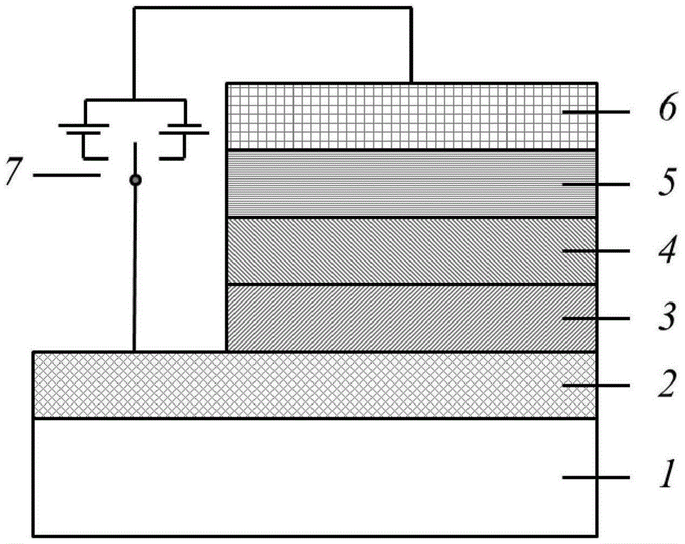
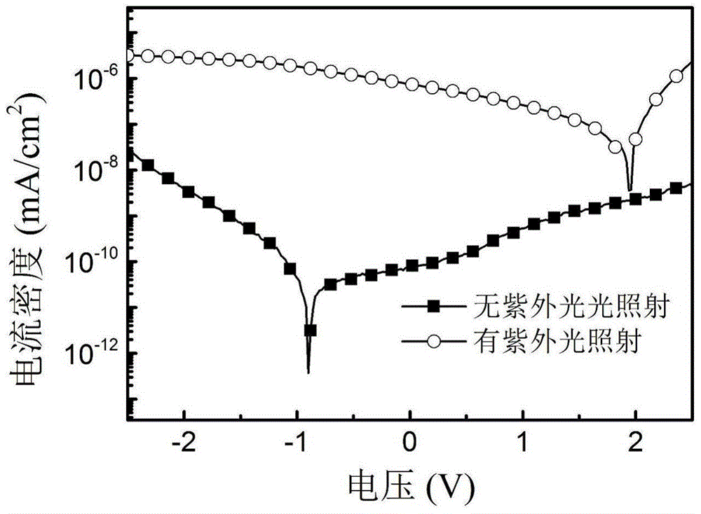
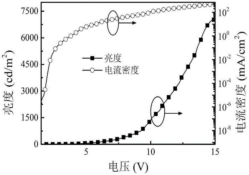
[0084] The hole transport layer material of the device is NPB, the organic active layer material is material 1, and the electron transport material is Alq 3 , The cathode layer is made of Mg:Ag alloy. The entire device structure is described as:

[0085] Glass substrate / ITO / NPB(15nm) / Material 1(15nm) / Alq 3 (20nm) / Mg:Ag(90nm)

[0086] The preparation method is as follows:

[0087] ①Use ethanol solution, acetone solution and deionized water to ultrasonically clean the transparent conductive substrate ITO glass, and dry it with dry nitrogen after cleaning. Wherein the ITO film on the glass substrate is used as the anode layer of the device, the square resistance of the ITO film is 10Ω / □, and the film thickness is 160nm.

[0088] ②The dried substrate was moved into a vacuum chamber, and the ITO glass was pretreated with low-energy oxygen plasma for 5 minutes under an oxygen pressure environment with an air pressure of 20Pa, and the sputtering power was 20W.

[0089] The treat...

Embodiment 2

[0094] The hole transport layer material of the device is NPB, the organic active layer material is material 2, and the electron transport material is Alq 3 , The cathode layer is made of Mg:Ag alloy. The entire device structure is described as:

[0095] Glass substrate / ITO / NPB(15nm) / Material 2(15nm) / Alq 3 (20nm) / Mg:Ag(90nm)

[0096] The fabrication process of the device is similar to that of Example 1.

Embodiment 3

[0098] The hole transport layer material of the device is NPB, the organic active layer material is material 3, and the electron transport material is Alq 3 , The cathode layer is made of Mg:Ag alloy. The entire device structure is described as:

[0099] Glass substrate / ITO / NPB(15nm) / Material 3(15nm) / Alq 3 (20nm) / Mg:Ag(90nm)

[0100] The fabrication process of the device is similar to that of Example 1.


PUM


Abstract

The invention discloses an organic dual-functional device and a preparation method thereof. The device comprises a transparent substrate, an anode layer, a hole transport layer, an organic active layer, an electron transport layer and a cathode layer. Under the drive of an applied forward voltage, the organic dual-functional device can achieve an electroluminescence function; and under the drive of an applied backward voltage, the device can achieve an ultraviolet detection function. The organic dual-functional device simultaneously has electroluminescence and ultraviolet detection dual-functions, has the characteristics of being high in efficiency, ultra-thin and integrated, and is simple in preparation technology, short in preparation time and low in cost.

Description

technical field [0001] The invention relates to the field of organic optoelectronics, in particular to an organic dual-function device and a preparation method thereof. Background technique [0002] Today, with the rapid development of science and technology, organic optoelectronic technology is a high-tech science developed rapidly as the inheritance and development of microelectronic technology. With the rapid development of materials science and electronic microelectronics, organic optoelectronic technology has been greatly developed, organic electroluminescent devices, organic photovoltaic solar cells, organic ultraviolet detectors, organic field effect transistors and other organic optoelectronic devices are rapidly developing. developing. Among them, organic electroluminescent devices have unique advantages in the field of solid-state lighting and flat panel display due to their advantages of light weight, high efficiency, self-luminescence, low power consumption, wid...

Claims


Application Information

Patent Timeline
Patent Type & Authority Applications(China)
IPC IPC(8): H01L51/00
CPCH10K85/6572
Inventor 于军胜周殿力王润蒋泉
Owner UNIV OF ELECTRONICS SCI & TECH OF CHINA
Why Eureka
Try Eureka