A Method of Suppressing the Propagation of Normally Connected Defects in Nano CMOS Circuits

A nano-defect technology, applied in the direction of logic circuits, logic circuits with logic functions, electrical components, etc., can solve the problems of uncontrolled signal transmission, affecting the logic function of the circuit, and speeding up the application process of CMOL circuits. Effects of Simplifying Constraints and Solving the Problem of Constantly Connected Defect Propagation

Active Publication Date: 2018-10-23
NINGBO UNIV
View PDF4 Cites 0 Cited by
  • Summary
  • Abstract
  • Description
  • Claims
  • Application Information

AI Technical Summary

Problems solved by technology

from image 3 It can be seen that unit D and unit C are always connected, and unit C and unit F are always connected. These constantly connected units transmit signals that are not necessarily transmitted to F to F. The programmable nano-diodes that are always connected make the signal transmission uncontrollable and affect The logic function of the circuit, how to reduce the influence of the constant connection defect on the logic function of the circuit is related to the application prospect of the nanometer CMOS circuit
At present, there is no effective method to suppress the propagation of normally connected defects in nano-CMOS circuits. Therefore, research on the method of suppressing the propagation of normally connected defects in nano-CMOS circuits can speed up the application process of CMOL circuits, which has strong practical significance.

Method used


Image

  • A Method of Suppressing the Propagation of Normally Connected Defects in Nano CMOS Circuits
  • A Method of Suppressing the Propagation of Normally Connected Defects in Nano CMOS Circuits
  • A Method of Suppressing the Propagation of Normally Connected Defects in Nano CMOS Circuits

Examples


Embodiment Construction

[0024] The present invention will be further described in detail below in conjunction with the accompanying drawings.

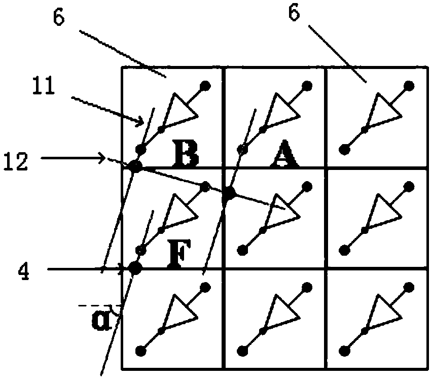
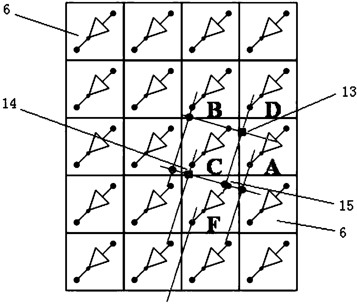
[0025] by image 3 Taking the nano-CMOS circuit structure with a size of 4*5 as shown as an example, the method for suppressing the propagation of the always-connected defect of the nano-CMOS circuit includes the following steps:

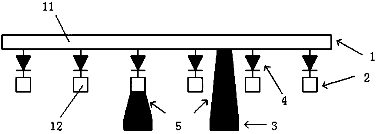
[0026] Define nanoscale CMOS circuit structures (see figure 1 ) includes an output nanowire layer 1, an input nanowire layer 2, several programmable nanodiodes 4 and several nanometer CMOS units 6, the output nanowire layer 1 and the input nanowire layer 2 are arranged at intervals up and down, and the output nanowire layer 1 consists of A plurality of parallel output nanowires 11, the input nanowire layer 2 is composed of a plurality of parallel input nanowires 12, any output nanowire 11 is vertically crossed with any input nanowire 12, and a programmable Nano diode 4; several nano CMOS units 6 are provided with a CMOS stack 3, ...


PUM


Abstract

The invention discloses a method for inhibiting propagation of a common defect of a nano CMOS circuit. Under the circumstance that in a manufacturing process of the nano CMOS circuit, it is inevitable to introduce a common connection defect in a programmable nano diode, which can lead to a wide propagation phenomenon of the common connection defect, the inventor analyzes a mode of action of the common connection defect of the programmable nano diode and a structural feature of the nano CMOS circuit, uses an inverter existing a CMOL circuit to generate a complementary signal, inputs the complementary signal to a nano CMOS unit which may propagate the common connection defect, inhibits the propagation of the common connection defect of the nano diode, simplifies the constraint of circuit mapping, increases the success rate of circuit mapping, and reduces the influence of the common connection defect on a logic function of the nano CMOS circuit, thereby effectively solving the problem of common connection defect propagation of the programmable nano diode of a nano CMOS circuit structure, and speeding up a practical process of a CMOL circuit structure.

Description

technical field [0001] The invention relates to a fault-tolerant mapping method of a nanometer CMOS circuit, in particular to a method for suppressing the propagation of the always-connected defect of the nanometer CMOS circuit. Background technique [0002] At present, the traditional CMOS process has reached 10-14 nanometers, and the further reduction of process nodes will reach the physical limit of silicon-based devices. The further reduction of the feature size of integrated circuits will bring many insurmountable challenges to the design of silicon-based integrated circuits: (1) photolithographic calibration becomes more difficult; (2) the generation of quantum effects makes the physical characteristics of transistors impossible control. For these reasons, the further development of silicon-based integrated circuits will encounter bottlenecks, and finding substitutes for silicon-based devices has become a research hotspot. [0003] Likharev and his colleagues propose...

Claims


Application Information

Patent Timeline
Patent Type & Authority Patents(China)
IPC IPC(8): H03K19/20H03K19/0948
CPCH03K19/0948H03K19/20
Inventor 夏银水陈定亨
Owner NINGBO UNIV
Why Eureka
Try Eureka