Method and apparatus for thermal mapping and thermal process control

A heat treatment device and controller technology, applied in semiconductor/solid-state device manufacturing, electrical components, circuits, etc., can solve problems such as different device performance, increased processing and manufacturing IC complexity, and no monitoring inhomogeneity

Active Publication Date: 2016-11-23
TAIWAN SEMICON MFG CO LTD
View PDF13 Cites 2 Cited by
  • Summary
  • Abstract
  • Description
  • Claims
  • Application Information

AI Technical Summary

Problems solved by technology

This scaling down also increases the complexity of handling and manufacturing ICs and requires similar developments in IC processing and manufacturing for the advancements to be achieved
In one example, when a thermal annealing process is applied to a

Method used


Image

  • Method and apparatus for thermal mapping and thermal process control
  • Method and apparatus for thermal mapping and thermal process control
  • Method and apparatus for thermal mapping and thermal process control

Examples


Embodiment Construction

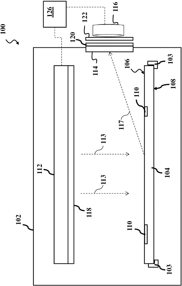
[0036] The following disclosure provides many different embodiments, or examples, for implementing the different features of the invention. Specific examples of components or configurations are described below to simplify the present invention. Of course, these are merely examples and not intended to be limiting. For example, in the description below, forming a first feature on or over a second feature may include embodiments in which the first feature and the second feature are formed in direct contact, and may also include embodiments in which the first feature and the second feature may be formed in direct contact. An embodiment in which the part forms an accessory part such that the first part and the second part are not in direct contact. Furthermore, the present invention may repeat reference numerals and / or letters in various instances. These repetitions are for simplicity and clarity and do not in themselves indicate a relationship between the various embodiments and...


PUM


Abstract

A thermal processing apparatus is provided in accordance with some embodiments. The thermal processing apparatus includes a heating source for transmitting incident radiation to a work piece having a circuit pattern formed on a front surface; a radiation sensor configured to receive light radiated from the front surface of the work piece; and a controller coupled to the radiation sensor, the controller being designed to control the heating source to reduce temperature variation of the work piece.

Description

[0001] cross reference [0002] This application is a continuation-in-part of US Patent Application Serial No. 12 / 789,816, filed May 28, 2010, the entire contents of which are hereby incorporated by reference. technical field [0003] The present invention generally relates to the technical field of semiconductors, and more particularly relates to a heat treatment device and method. Background technique [0004] The semiconductor integrated circuit (IC) industry has undergone rapid development. Technological advances in IC materials and design have produced multiple generations of ICs, each with smaller and more complex circuits than the previous generation. These advances have increased the complexity of handling and manufacturing ICs, and similar developments in IC processing and manufacturing are required for advancements to be realized. In the course of IC evolution, functional density (ie, the number of interconnected devices per chip area) generally increases, while ...

Claims


Application Information

Patent Timeline
IPC IPC(8): H01L21/324H01L21/66
Inventor 蔡俊雄陈科维
Owner TAIWAN SEMICON MFG CO LTD
Why Eureka
Try Eureka