Shift-register circuit and display device containing same
A shift register and circuit technology, applied in static memory, digital memory information, instruments, etc., can solve the problem of reduced operating margin of shift register circuits, and achieve the effect of improving operating margin
- Summary
- Abstract
- Description
- Claims
- Application Information
AI Technical Summary
Problems solved by technology
Method used
Image

Examples
no. 1 Embodiment approach >
[0076] (Configuration of liquid crystal display device)
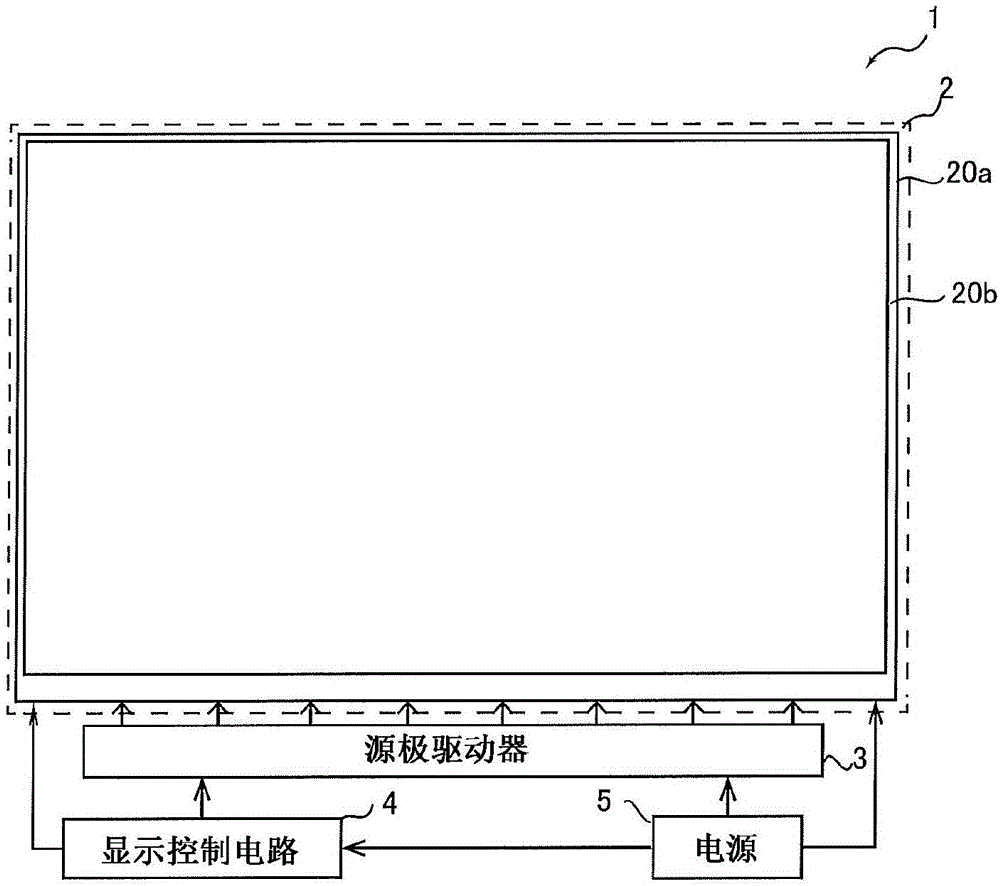
[0077] figure 1 It is a schematic diagram showing the schematic configuration of the liquid crystal display device of the present embodiment. The liquid crystal display device 1 has a display panel 2 , a source driver 3 , a display control circuit 4 and a power supply 5 . The display panel 2 has an active matrix substrate 20a, a counter substrate 20b, and a liquid crystal layer (not shown) sandwiched between these substrates. exist figure 1 Although not shown, a pair of polarizing plates are provided to sandwich the active matrix substrate 20a and the counter substrate 20b. A black matrix, color filters of three colors of red (R), green (G), and blue (B), and a common electrode (both not shown) are formed on the counter substrate 20b.
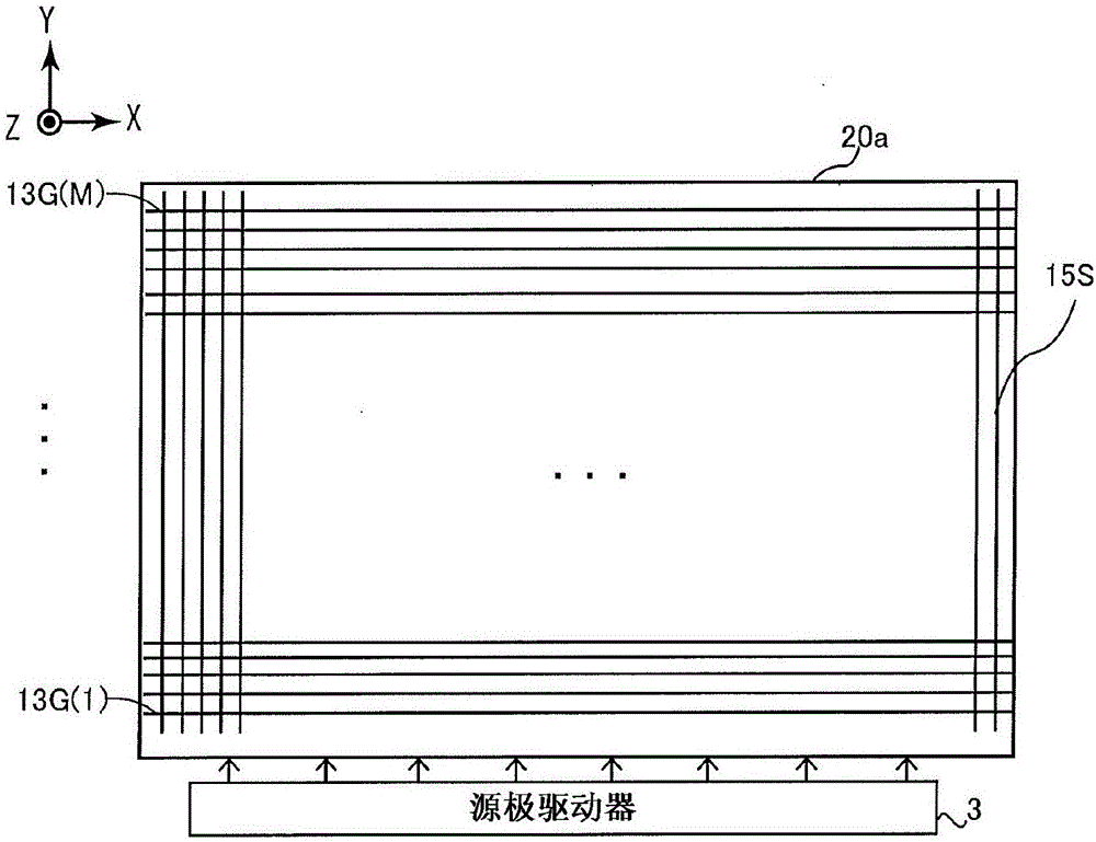
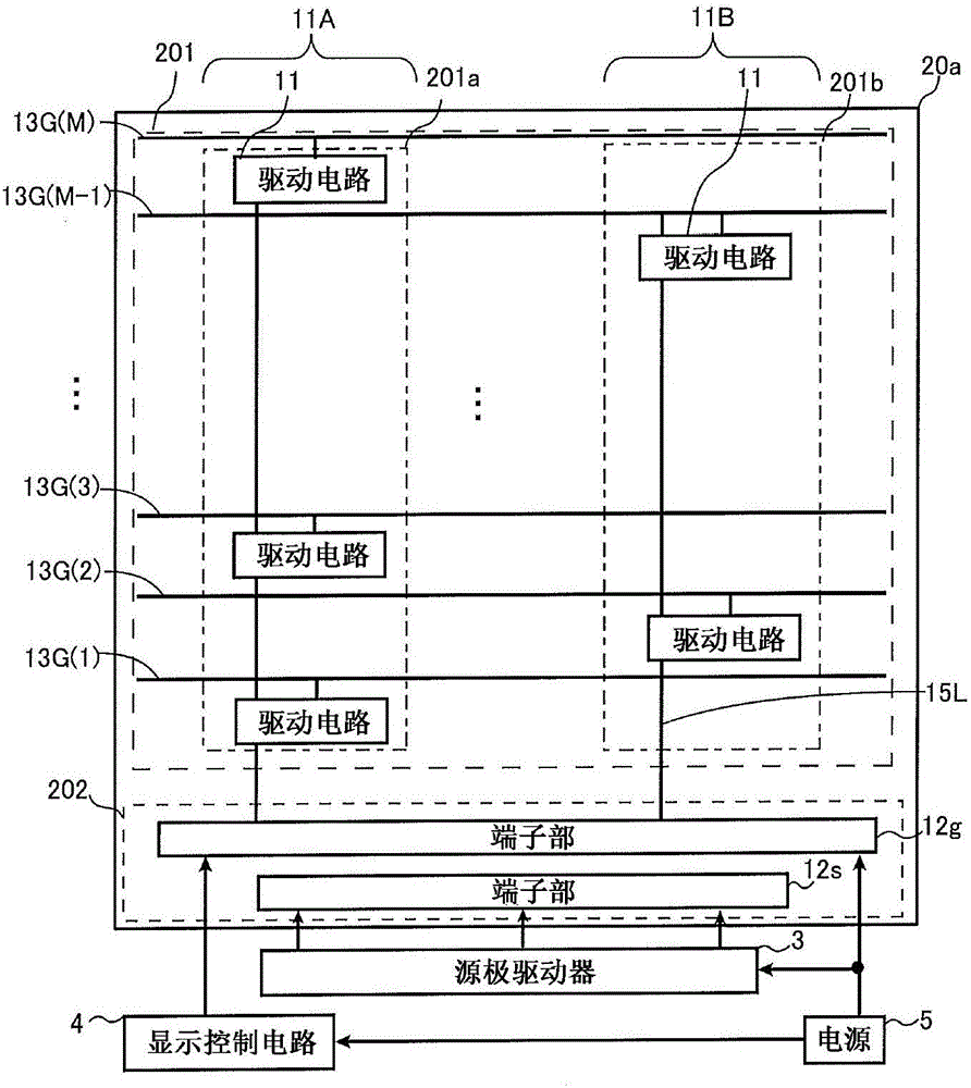
[0078] Such as figure 1 As shown, the active matrix substrate 20a is electrically connected to the source driver 3 formed on the flexible substrate. The display control circuit 4 i...
no. 2 Embodiment approach >
[0147] In the above-mentioned first embodiment and its application examples, an example in which the decrease in the precharge voltage of netA is suppressed and the operating margin of the gate driver is improved has been described. The reason for the decrease in the operating margin of the gate driver is that the potential of netA is not sufficiently lowered when the gate line is switched to the non-selection period. In particular, when the gate driver is arranged in the display area, it may not be possible to reliably pull down netA due to the influence of parasitic capacitance generated between elements such as the source line 15S and the wiring 15L arranged in the display area. to low level. In this embodiment, an example will be described in which the potential of netA is pulled down more reliably when the gate line is brought into the non-selected state in order to increase the operating margin of the gate driver. Configurations different from those of the first embodim...
no. 3 Embodiment approach >
[0164] In the above-mentioned second embodiment, in order to improve the operating margin of the gate driver, netA of another drive circuit was connected to the gate terminal of TFT-K functioning as a gate voltage discharge unit, and the TFT-K An example of increased drive. In this embodiment, discharge of the gate line when the gate line transitions to a non-selection period is strengthened to improve the operating margin of the gate driver. Hereinafter, configurations different from those of the second embodiment will be described.
[0165] (circuit configuration)
[0166] Figure 16 It is a diagram illustrating an equivalent circuit of the drive circuit 112 of the present embodiment. Such as Figure 16 As shown, in the drive circuit 112(n) for driving the gate line 13G(n), the gate terminal of the TFT-K for pulling down the potential of netA(n) is connected to the gate line 13G(n+2). , the drain terminal is connected to netA(n), and the source terminal is input with th...
PUM
 Abstract
Description
Claims
Application Information
 - R&D Engineer
- R&D Manager
- IP Professional
- Industry Leading Data Capabilities
- Powerful AI technology
- Patent DNA Extraction
Browse by: Latest US Patents, China's latest patents, Technical Efficacy Thesaurus, Application Domain, Technology Topic.
© 2024 PatSnap. All rights reserved.Legal|Privacy policy|Modern Slavery Act Transparency Statement|Sitemap