Manufacturing method of semiconductor integrated circuit device

A technology of integrated circuits and manufacturing methods, applied in the direction of semiconductor/solid-state device manufacturing, circuits, electrical components, etc., can solve the problems of thinning, adverse effects of transistor characteristics, deterioration of gate insulating film reliability, etc., to prevent deterioration of characteristics. Effect

Inactive Publication Date: 2006-01-11
SANYO ELECTRIC CO LTD
View PDF1 Cites 0 Cited by
  • Summary
  • Abstract
  • Description
  • Claims
  • Application Information

AI Technical Summary

Problems solved by technology

[0006] However, when the above-mentioned etching and thermal oxidation are repeated many times, the reliability of the gate insulating film will deteriorate, or the field oxide film will be etched and thinned, which will adversely affect the characteristics of the transistor.

Method used


Image

  • Manufacturing method of semiconductor integrated circuit device
  • Manufacturing method of semiconductor integrated circuit device
  • Manufacturing method of semiconductor integrated circuit device

Examples


Embodiment Construction

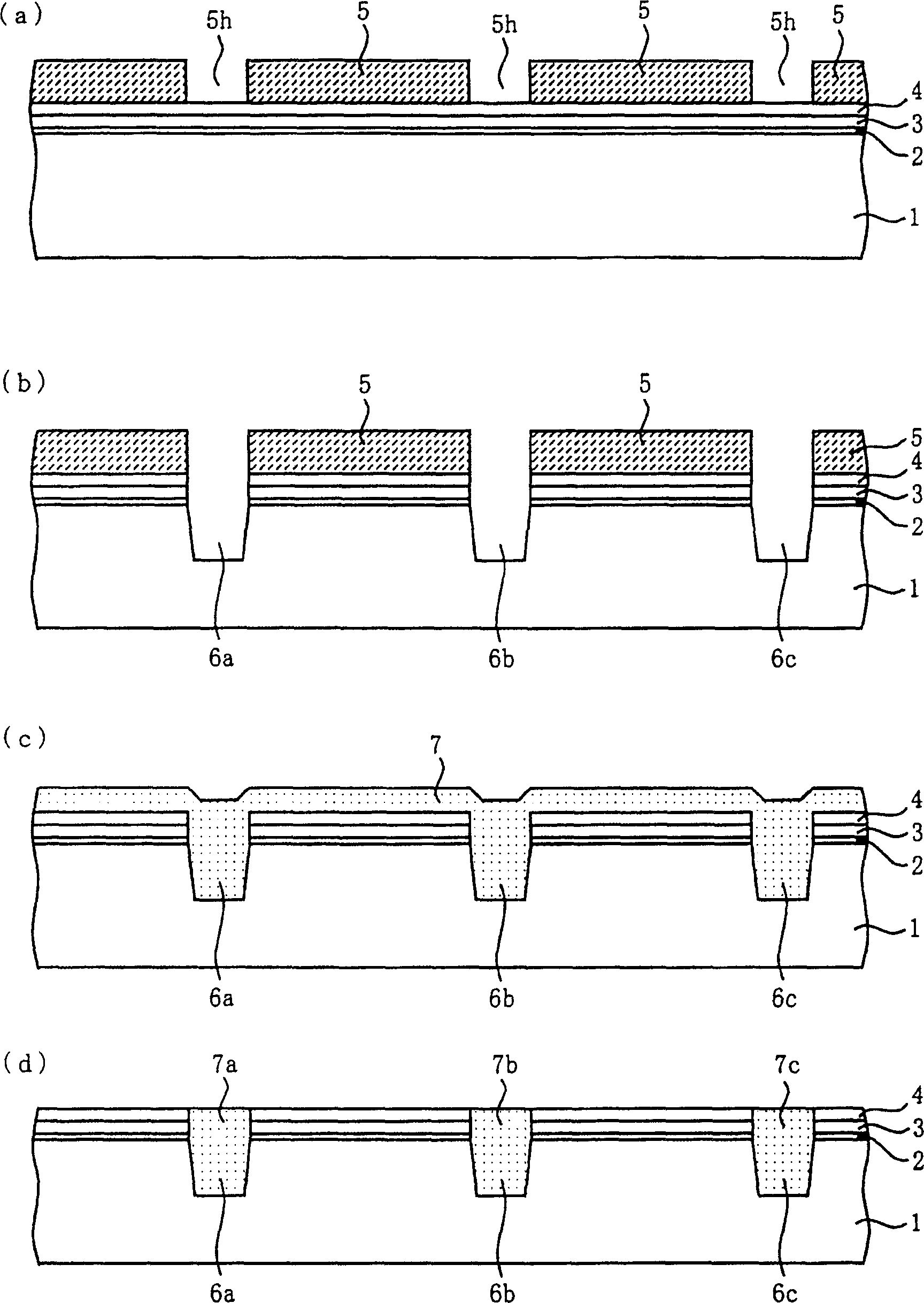
[0017] A method of manufacturing a semiconductor integrated circuit device according to an embodiment of the present invention will be described below with reference to the drawings. First, a reference example for comparison with the manufacturing method of the semiconductor integrated circuit device of the embodiment will be described.

[0018] Such as figure 1 As shown in (a), on the surface of the P-type silicon substrate 1, about 10 nm of SiO is formed by thermal oxidation. 2 Membrane 2 (Silicon Dioxide Membrane). Then, on SiO 2 On the film 2, a polysilicon film 3 with a film thickness of about 50 nm and a Si film with a film thickness of 120 nm are formed by CVD. 3 N 4 film4. Then, at Si 3 N 4 A photoresist layer 5 having a plurality of openings 5 ​​h is formed on the film 4 .

[0019] Then, if figure 1 As shown in (b), the Si exposed at the opening 5h is sequentially etched using the photoresist layer 5 having a plurality of openings 5h as a mask. 3 N 4 Film 4...


PUM


Abstract

The invention is directed to a semiconductor integrated circuit device having a plurality of gate insulation films of different thicknesses where reliability of the gate insulation films and characteristics of MOS transistors are improved. A photoresist layer is selectively formed on a SiO2 film in first and third regions, and a SiO2 film in a second region is removed by etching. After the photoresist layer is removed, a silicon substrate is thermally oxidized to form a SiO2 film having a smaller thickness than a first gate insulation film in the second region. Then, the SiO2 film in the third region is removed by etching. After a photoresist layer is removed, the silicon substrate is thermally oxidized to form a SiO2 film having a smaller thickness than a second gate insulation film in the third region.

Description

technical field [0001] The present invention relates to a method of manufacturing a semiconductor integrated circuit device, and more particularly, to a method of manufacturing a semiconductor integrated circuit device having a plurality of gate insulating films having different film thicknesses. Background technique [0002] In recent years, in order to achieve higher integration and higher functionality of semiconductor integrated circuit devices, system LSIs incorporating memories such as flash memories and high withstand voltage MOS transistors have been developed. [0003] In such a semiconductor integrated circuit device, when a low-voltage MOS transistor and a high-voltage MOS transistor are integrated on the same semiconductor substrate, the low-voltage MOS transistor is miniaturized by forming a thin gate insulating film, while the high-voltage MOS transistor is miniaturized. In order to secure a high withstand voltage of the gate insulation of a voltage-resistant M...

Claims


Application Information

Patent Timeline
Patent Type & Authority Applications(China)
IPC IPC(8): H01L21/8234
CPCH01L21/823481H01L21/823462
Inventor 尾关和之塚田雄二
Owner SANYO ELECTRIC CO LTD
Why Eureka
Try Eureka